10 Questions with Aaron Stein
interview with a CFN Scientist
December 28, 2012
Before 3D printers began grabbing headlines and heralding new kinds of creation, top scientists were already printing fully functional materials on scales spanning just billionths of a meter.
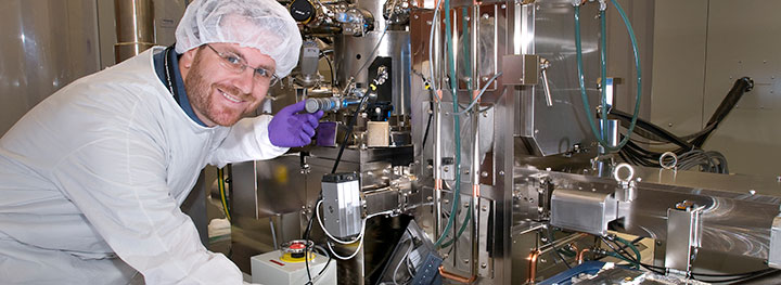
Brookhaven Lab physicist Aaron Stein specializes in electron beam lithography (EBL), a technique that uses advanced machinery to draw nanoscale patterns into a wide range of materials. Applications for the technique include everything from advanced electronics to x-ray-focusing lenses, and Stein’s expertise puts him in constant collaboration with the users and staff at the Center for Functional Nanomaterials. Stein joined the CFN staff as the first official hire almost exactly 10 years ago, before the facility even existed. Since then, the number of users grew dramatically, cutting-edge suites of instruments were added, and the research possibilities flourished.
What attracts you to a new experiment or potential collaboration?
First and foremost, of course, I look for projects that are interesting from a scientific perspective: Does the science make sense and is it worthy of the time it will take? Often I’ll wonder if I could make the problem and the proposed solution sound exciting to a non-scientific friend. Beyond that, I am very interested in projects that will push what is possible in terms of nanofabrication, from working in smaller and smaller dimensions to testing new classes of materials. I’m not as interested in just making a new set of gold electrodes on silicon substrates—although that can certainly drive interesting research areas.
Published papers are often just about the results of testing the final nanostructures or devices, but a lot of the essential effort goes into perfecting the fabrication. It’s a bit of an under-appreciated art, actually.
What sorts of experiments are ideally suited for e-beam lithography?
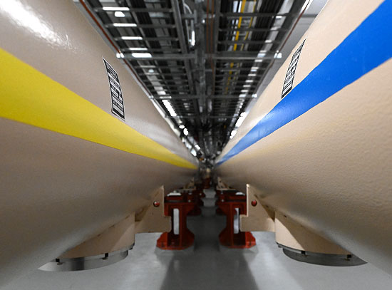
Any time a structure needs to be made on the nanoscale, e-beam is a top candidate. Using a state-of-the-art e-beam writer like the one at CFN allows for high-resolution features and for large areas to be covered with arbitrary geometries on both standard and non-standard substrate types and sizes.
Because of the size scales involved and the precision needed for pattern placement, a lot of optics-related science requires e-beam lithography, ranging from photonic devices operating over a range of wavelengths to x-ray optics. Studying materials such as nanotubes, nanowires, or graphene can also use EBL to fabricate test devices with exact proportions and alignments.
Why is specialized training and experience so essential in your field?
EBL is a classic easy-to-learn, lifetime-to-master kind of activity. There is a rote, algorithmic quality to just making the machine work that can be taught to almost anyone—but at the same time, there are dozens of factors that go into a successful e-beam process that one only encounters through first-hand experience. Ultimately, things go wrong—because of new materials, something unexpected in the chemistry, or because what worked on a Monday in December doesn’t seem to do the trick on a Wednesday in July. Over time you get a sense for some (but never all) of the challenges that can arise, and you start to work out solutions that might never make it into any publication. Gaining experience and interacting with other people doing similar things is absolutely essential as you leave the beaten path of e-beam lithography.
CAD plays an essential role in your process—what problems do you work through with that software?
When you start pushing the limits of EBL, CAD and pattern fracture components start to become very important. First, I try to optimize writing time. EBL is a serial process, and as layout designs get larger and more elaborate, any strategy that can be employed to reduce the exposure time is beneficial. Second, I have to consider pattern fidelity, or how closely the exposure matches the design, which involves translating program pixels into the real world of e-beam parameters. Finally, proximity effect correction, or PEC, plays an important role in pattern design and conversion. Feature size and density, e-beam resist, and substrate type affect the local and global dose in complicated ways.
Although it shouldn’t surprise me, I still get amazed at how small tweaks to a process can generate such wildly different results. The nanosphere is a fascinating place!
How does e-beam lithography translate into material etching?
The trick is to work backwards from the final product. You need an appropriate mask for an etch to work, and that’s dependent on the material, pattern depth, and the lateral dimensions of the features. You also need to consider whether the mask will be etched or made by material deposition. From there you determine what resist you will use, and then ensure design compatibility. And this, of course, is all repeated over and over again.
One long-running project of mine—fabrication of x-ray lenses—requires a deep silicon etch of 50-100 micrometers. Over the years we’ve gone through many different masks to allow us to etch that deeply, including silicon dioxide, aluminum nitride, and chromium, and each step introduced new wrinkles in both EBL exposures and materials processing.
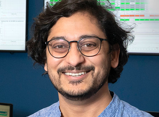
Aaron Stein
What are some of the nanofabrication obstacles that you’re currently facing?
One project requires working with silicon nitride membranes, which can be quite fragile. I have to come up with new techniques for handling and processing these membranes during the many fabrication steps just to ensure that we have some structure still standing when all is said and done. Another project involves etching an aluminum film that’s incompatible with some of the negative resists and chemicals I would normally use for that type of etch process, so I had to engineer a solution with a positive resist and lift-off. That change introduced its own set of problems that limited the ultimate size of the features I wanted to make, but I’m sure we’ll work through it.
What’s one major advantage of working at CFN?
We obviously have all these great instruments, but the human factor is even more important. When you need to use a transmission electron microscope, for example, you can walk over to a dedicated expert who actually pushes the scientific possibilities of that instrument. This isn’t just someone training you; this is someone who will work with you in a real, ongoing collaboration.
In my group, I often work closely with Ming Liu, an etching expert here at CFN. Being able to talk through a problem with him and really lean on that expertise raises the caliber and efficiency of our work.
What new experimental horizons are you looking forward to in 2013?
I’m most excited by problems that push the envelope of what can be done with EBL and related nanofabrication processes. Along those lines, I hope to delve deeper into the machine and the processes themselves. How can we use PEC to fabricate more challenging structures? What kind of metrology techniques can be developed to characterize the limits of the EBL machine? My next great nanofabrication challenge may be lurking just around the corner and out of sight for the moment, so who knows what I’ll actually end up working on in the coming year.
Do you have any advice for incoming users or new hires?
Sometimes grad students and postdocs have an insular feeling as a group, which can become kind of competitive or closed off. This is the opposite attitude to have at the CFN—you’re surrounded by brilliant potential collaborators, and that’s part of the beauty of working at a user facility like this.
Also, I’d say to be careful about the expectations you have for your research timetable. Students come in thinking that they’ll make some new device in just a few months and then spend the next five years collecting data on its properties. But in reality, you’ll probably spend five challenging years on fabrication, and the last few months taking as much data as possible. That’s almost inevitably what happens.
You have two young kids - what do they think about what you do?
I think they like being able to tell their friends that their dad is a scientist at Brookhaven. Maybe they’ll take science more seriously, and at the very least they know that this kind of career is in the realm of possibility.
I went and spoke at my daughter’s school recently, and that was really exciting. I doubt that the kids really understood electron beam lithography, but they seemed interested and I got these great cards and questions back. One of the kids asked, “What if zombies took over the world? What are you doing to deal with that?” Maybe my research won’t save us from zombies, but you really never know what exciting things we’ll discover.
2012-3568 | INT/EXT | Newsroom