10 Questions with Kevin Yager
interview with a CFN Scientist
December 11, 2013
Kevin Yager
The next-generation of catalysts, solar cells, and microchips will be built and manipulated with precision stretching from the macroscopic to the atomic. There are two principle elements to advancing nanoscale fabrication: construction and characterization. Kevin Yager, a staff scientist at Brookhaven Lab’s Center for Functional Nanomaterials (CFN), happens to specialize in both. Yager’s expertise includes making materials through meticulously guided self-assembly, and probing nanoscale structures with x-ray scattering.
How does x-ray scattering reveal details spanning just billionths of a meter?
Visible light has a wavelength that is much larger than the nanomaterials we explore at CFN, making it impossible to directly visualize them. X-rays, however, have very short wavelengths, making them ideal for measurements at the atomic and nanoscale. I specialize in x-ray scattering, where an intense and focused x-ray beam is fired through a sample. The x-rays diffract off the atomic and molecular structures, and we measure the angles of that scattering with sophisticated detectors. We end up with these very complex and inscrutable diffraction patterns.
How do you deduce actual structures from the scattering patterns?
 enlarge
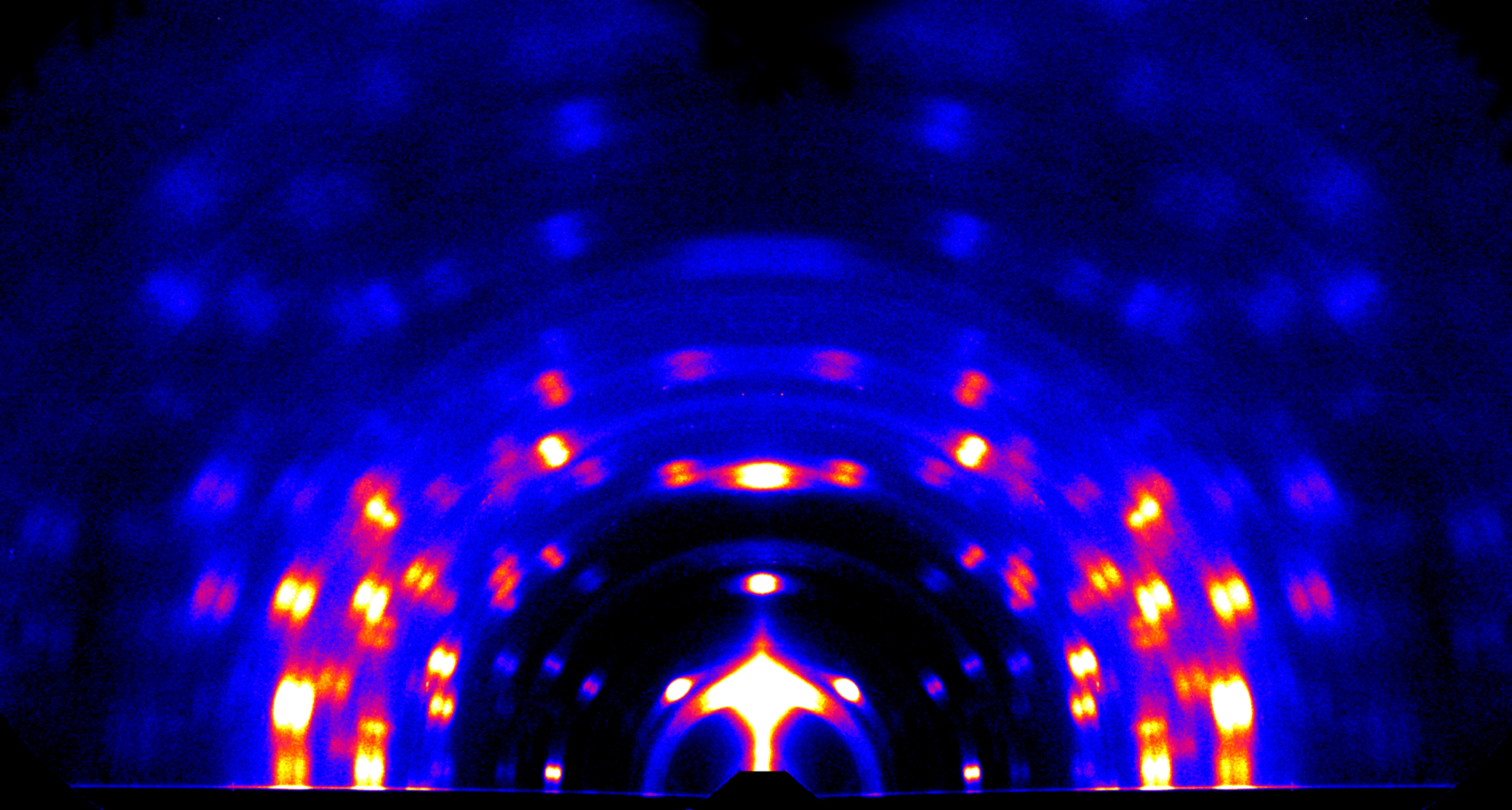
Example of a wide-angle x-ray scattering and diffraction pattern obtained from a thin film of organic semiconductor.
That’s one of the trickiest parts of my work, and it combines quite a bit of both computer science and theoretical modeling. The diffraction pattern is a far cry from being a direct representation. You get features like peaks, rings, or halos. It’s almost the Fourier transform of the samples’ structure, except that since we’ve only measured the amplitude and not the phase of the scattering, we cannot invert the data to obtain the structure. Instead, we develop mathematical models to fit the data, and thereby infer the real-space structure. Different kinds of nanostructures thus require different kinds of models. In fact, I often develop new models for specific user experiments, and that’s part of what makes the work so interesting.
There are many different kinds of x-ray scattering experiments, tuned to probe different structures at different scales. For instance, wide-angle scattering can reveal molecular structure, molecular packing, and atomic spacing, while small-angle scattering can address nanoscale structure, phase separation of polymers, lithographic patterns, particle orientations, and so on. In my own research and my work with users, I take advantage of a whole suite of x-ray scattering techniques in concert.
How does x-ray scattering compare to or complement other imaging techniques?
One major difference with electron microscopy, for example, is that x-ray scattering measures the average structure over large areas. For example, this lets you know whether your nanostructures are truly uniform over an entire device, so it’s obviously of importance for industrial applications. We’re resolving atomic and nanoscale structures, but we’re doing it globally rather than locally.
X-ray scattering also works well for in situ experiments. For example, probing materials in solutions or under conditions very similar to actual operational environments. This is key when it comes to advancing energy technology. Electron microscopy—incredibly useful in its own right—usually requires high vacuum, whereas we can tweak and test different conditions and get crucial real-time performance data.
How does your research translate into practical applications?
 enlarge
Example of a nanostructured thin film, obtained using a self-assembled block-copolymer film as an etch mask (generated with CFN collaborators Dan Johnston and Chuck Black).
As just one example, I recently worked on a project to improve the performance of organic photovoltaics (OPV)—solar cells made out of polymers rather than inorganic materials like silicon. It turns out that these OPV materials (organic semiconductors) exhibit anisotropic conduction, which is to say that their conductivity depends on which direction you probe. So, to maximize solar conversion efficiency, we wanted to control the orientation of the organic semiconductors within the device.
So we infiltrated the OPV polymer—in this case a compound called polythiophene—into custom-made nanoporous substrates. Using a combination of wide- and small-angle x-ray scattering, we found that our nanoconfinement could be used to randomize or align the orientation distribution. This allowed us to improved charge transport, which in principle will improve solar cell performance.
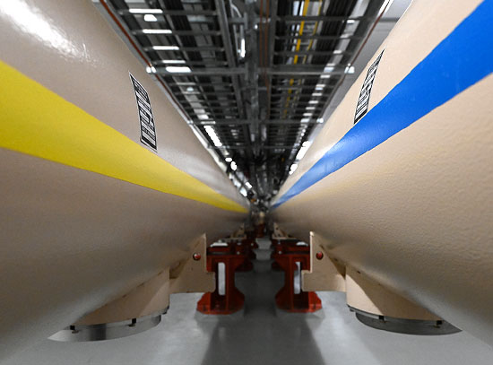
You must need an exceptional light source to for x-ray scattering – how does NSLS factor into your research?
NSLS is absolutely essential. The intense and highly collimated x-ray beams I need can only be found at a few facilities in the world, and I’m lucky to have one of those right across the street. I co-manage beamline X9 at NSLS, where I work with users to prepare samples, install them at the beamline, run the scattering experiment, and then interpret the data.
 enlarge
Nanoparticle superlattices (schematic in the foreground) represent a new class of nanomaterials being investigated at CFN and elsewhere. Their nanoscale structural order gives rise to well-defined small-angle scattering peaks (data in the background). Quantitative analysis of this kind of data required the development of a new scattering model.
What effect will the National Synchrotron Light Source II have on your research when it comes online in 2015?
NSLS-II will push my work into new frontiers. The higher x-ray flux and coherence will offer experimental capabilities unavailable anywhere else on the planet. We will be able to focus x-rays much more tightly than ever before. Whereas we talk in terms of ‘microbeams’ at NSLS, we’ll be able to generate nanoscale beams at NSLS-II that will enable powerful new techniques like materials mapping. Biological samples, for example, are heterogeneous, meaning that the structural averages over larger areas provide an incomplete picture. At NSLS-II, we can pin down structure on specific parts of the tissue and link it back to function much more precisely. The same is true of industrial materials: by finely probing structural heterogeneity, we will be able to greatly enhance material performance.
What’s the benefit to users of working with CFN staff experts?
One of the things I enjoy most about my job is the way I can facilitate an experiment all the way from conception to publication. New and prospective users will contact me to discuss their experiments, and I can help shape the research plan from an early stage. They sometimes send me samples to do feasibility tests at NSLS, which helps establish both the timetable and parameters of the proposed project. After the initial tests and discussions, I train users, both students and more senior scientists, on how to use the beamline and run their own experiments—and they can take that education to other light sources around the world. I’m also available to help the users with challenging data interpretation.
Personally, a huge thrill for me is in developing new and untested techniques to answer the questions users bring to CFN. You only get that kind of adaptability from experts who can improvise when established methods aren’t effective. And that experience isn’t unique to x-ray scattering or self-assembly—this is the appeal of the CFN research community. Users come here and get access to this confluence of scientific expertise and engineering talent in electron microscopy, nanofabrication, lithography, and so on, not to mention the other resources at Brookhaven Lab.
You mentioned developing new techniques – can you give an example?
 enlarge
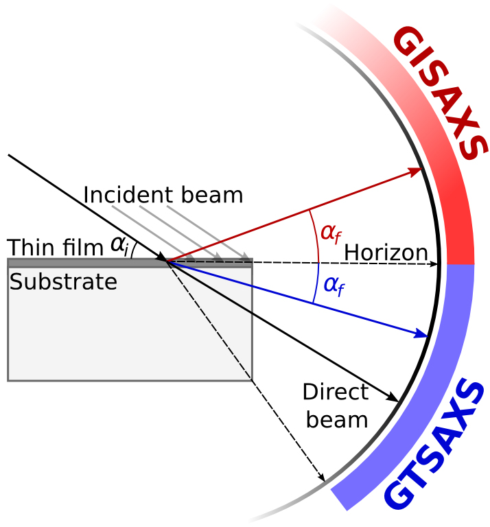
Geometry for a new x-ray scattering technique: Grazing-incidence Transmission Small-Angle X-ray Scattering (GTSAXS). By focusing an x-ray beam on the edge of a sample, the undistorted sub-horizon scattering can be measured. (Developed in collaboration with Xinhui Lu and Ben Ocko.)
I recently worked with Brookhaven colleagues to discover a new scattering geometry called Grazing-Transmission Small Angle X-ray Scattering (GTSAXS). A typical grazing-incidence experiment suffers from reflection and refraction effects, which distort the data and create a kind of image ghosting that complicates structural interpretations. We developed a technique where we focus the x-ray beam on the edge of the sample, so that the x-rays could exit rather than bouncing off the substrate, giving us much cleaner data. The discovery itself was actually a serendipitous accident owing to a misaligned sample, but we immediately recognized the experimental potential in the data.
What was your path to joining Brookhaven Lab and CFN?
I’ve always been passionate about science. I remember back in seventh grade, I enthusiastically presented a book report on nanotechnology to my class. Perhaps not surprisingly, my classmates were not nearly as excited. But now I’m realizing my dream of developing nanoscience. I received my PhD in chemistry from McGill University in Montreal and then completed my postdoc work doing neutron scattering at the National Institute of Standards and Technology—that’s where I discovered the collaborative, large-scale environment of national labs. I have always wanted to combine computer science and programming with physical experimentation, and that’s part of why my work at CFN is such a perfect fit.
What keeps you interested and engaged in your research?
CFN changes so much, year to year. We keep advancing the state-of-the-art, pushing technical boundaries, and moving into uncharted scientific territory. That sounds grandiose, I know, but it’s true. Our mission focuses in part on energy-related research, but we have a quite a bit of freedom and latitude to follow our passions and go where the science leads us. Every day that I come into the lab, some aspect of the work I do has never been done before. The challenges are new and complex, and the rotating cast of users keeps us all on our toes.
Kevin Yager, a scientist at Brookhaven Lab's Center for Functional Nanomaterials, discusses his research on materials spanning just billionths of a meter. Yager specializes in making new materials through meticulously guided self-assembly and probing nanoscale structures with a technique called x-ray scattering.
Featured Publications
Yager, K.G.; Zhang, Y.; Lu, F.; Gang, O. “Periodic lattices of arbitrary nano-objects: modeling and applications for self-assembled systems” J. Appl. Cryst. 2013, 47, in press.
Lu, X.; Yager, K.G.; Johnston, D.; Black, C.T.; Ocko, B.M. "Grazing-incidence transmission X-ray scattering: surface scattering in the Born approximation" Journal of Applied Crystallography 2013, 46, 165–172.
Johnston, D.E.; Yager, K.G.; Nam, C.-Y.; Ocko, B.M.; Black, C.T. "One-Volt Operation of High-Current Vertical Channel Polymer Semiconductor Field-Effect Transistors" Nano Letters 2012, 8, 4181–4186.
Allen, J.E.; Yager, K.G.; Nam, C.-Y.; Ocko, B.M.; Black, C.T. "Enhanced charge collection in confined bulk heterojunction organic solar cells" Applied Physics Letters 2011, 99, 163301.
2013-4510 | INT/EXT | Newsroom