Role of Size and Defects in Ultrafast Broadband Emission Dynamics of ZnO Nanostructures
July 8, 2014
What Is The Scientific Achievement?
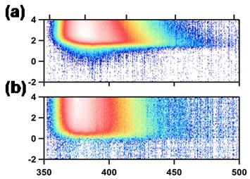
Figure 1: Broadband sub-ps transient emission spectra in (a) nanostructures reveal the presence of a large number of defects as compared to (b) bulk ZnO that lead to enhanced recombination. Our ultrafast spectrometer allowed us to record short-lived emission in the ultraviolet and visible range, and is optimized to allow us to probe emission dynamics under low light fluence conditions that are relevant for solar applications. Among other phenomena, we directly observed the presence of localized exciton states, which led to a low energy emission tail and a delay in the onset of fluorescence.
Understanding how the nanoscale affects a material’s optical behavior in the ultrafast regime is vital for telecommunications and energy-conversion technologies. This work investigates how small changes in the preparation of zinc oxide (ZnO), a prototypical wide bandgap semiconductor, can dramatically affect its light emitting properties. Recombination processes were monitored by utilizing a newly developed, high-sensitivity, sub-picosecond accuracy (10-12 seconds), transient broadband (> 2 eV) emission spectrometer. By investigating different geometries, including bulk, nanowires, and nanospheres (diameter ~ 40 nm), the presence of defects was demonstrated to dominate over geometrical consideration until the material quality is sufficiently high. Defects in the material led to localized excitonic states—not observed previously due to their short lifetimes—and modified the overall nanoscale carrier dynamics. The precise arrangement of atoms within the material without imperfections (defect-free) was found to precede any other consideration. The presence of defects created local perturbations that lived for a short duration and affected the overall dynamics and, thus, the performance of a device.
Why Does This Matter?

Figure 2: Visible-UV LED operates at low powers and optoelectronic circuits with ultrafast speeds when based on efficient nanoscale materials
Resolving sub-ps broadband emission in wide-bandgap nanomaterials is vital to understand recombination processes, which are important for optoelectronics and energy-related technologies. Within the size regime above electronic quantum confinement, crystal quality rather than dimensionality dictates the overall charge carrier dynamics.
What Are The Details?
- CFN Capabilities: A spectrometer that probe light emitted from nanomaterials with picosecond resolution (10-12 s) was built in the Advanced Optical Spectroscopy Facility.
- Achieving a high material quality is as important as controlling its size and dimensionality—bulk, nanosphere, nanowire—for optoelectronic and photonic applications.
Publication Reference
Role of Size and Defects in Ultrafast Broadband Emission Dynamics of ZnO Nanostructures
Kannatassen Appavoo, Mingzhao Liu, Matthew Y. Sfeir
Center for Functional Nanomaterials, Brookhaven National Laboratory, Upton, New York 11973, USA
Applied Physics Letters 104 (13), 133101 (2014)
Enhanced broadband ultrafast detection of ultraviolet emission using optical Kerr gating
Kannatassen Appavoo and Matthew Y. Sfeir
Center for Functional Nanomaterials, Brookhaven National Laboratory, Upton, New York 11973, USA
Rev. Sci. Instrum. 85, 055114 (2014)
Acknowledgment of Support
Research is carried out at the Center for Functional Nanomaterials, Brookhaven National Laboratory, which is supported by the U.S. Department of Energy, Office of Basic Energy Sciences, under Contract DE-AC02 98CH10886. The authors thank C.T. Black and A. Cook for helpful discussions, and X. Liu and V. Menon for providing the ZnO nanospheres sample.
2014-5038 | INT/EXT | Newsroom