Drawing at the One-Nanometer Length Scale
May 23, 2017
What is the scientific achievement?
CFN scientists have adapted a state-of-the-art electron microscope for lithography in order to achieve unprecedented one nanometer resolution —i.e., at the single-molecule level. These results are a significant improvement over the previous resolution limits of electron-beam lithography, a widely-used nanofabrication technique.
Why does this achievement matter?
These results demonstrate the importance of both the texture's characteristic feature size and shape on its antifogging ability.
What are the details?
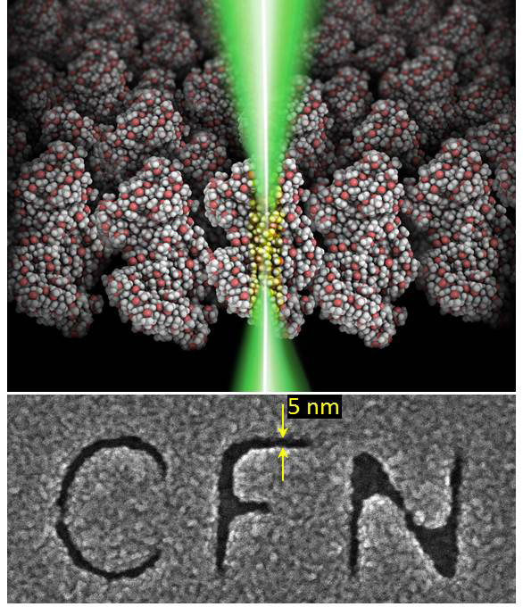
 enlarge
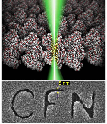
Top: Illustration of a focused electron beam (green) shining through a polymeric film (round particles are atoms of the film). The glowing area indicates the feature to be fabricated at the molecular length scale. Bottom: An arbitrary design printed at single-digit nanometer dimensions.
The ability to pattern materials at ever-smaller sizes—using electron-beam lithography (EBL), in which an electron-sensitive material is exposed to a focused beam of electrons, is driving advances in nanotechnology. When the feature size of materials is reduced from the macroscale to the nanoscale, individual atoms and molecules can be manipulated to dramatically alter material properties, such as color, chemical reactivity, electrical conductivity, and light interactions. In the ongoing quest to pattern materials with ever-smaller feature sizes, scientists at the Center for Functional Nanomaterials (CFN)—a U.S. Department of Energy (DOE) Office of Science User Facility at Brookhaven National Laboratory— have recently set a new record. Performing EBL with a state-of-the-art scanning transmission electron microscope (STEM), they have patterned thin films of the polymer poly(methyl methacrylate), or PMMA, with individual features as small as one nanometer (nm), and with a spacing between features of 11 nm, yielding an areal density of nearly one trillion features per square centimeter. The team's patterned PMMA films can be used as stencils for transferring the drawn single-digit nanometer feature into any other material. In this work, the scientists created structures smaller than 5 nm in both metallic (gold palladium) and semiconducting (zinc oxide) materials. Their fabricated gold palladium alloy features were as small as six atoms wide. This technique opens up many exciting materials engineering possibilities, tailoring properties closer to the atomic scale. The CFN we will soon be offering this first-of-a-kind nanoscience tool to users from around the world.
CFN Capabilities:
CFN Electron Microscopy and Nanofabrication Facilities were used for nanostructure fabrication, processing, and imaging.
Publication Reference
Vitor Riseti Manfrinato, Aaron Stein, Lihua Zhang, Chang-Yong Nam, Kevin G Yager, Eric A Stach, Charles T Black, Aberration-Corrected Electron Beam Lithography at the One Nanometer Length Scale, Nano Letters 17 (2017).
DOI: 10.1021/acs.nanolett.7b00514
Acknowledgement of Support
Research carried out at the Center for Functional Nanomaterials, which is supported by the U.S. Department of Energy, Office of Basic Energy Sciences, under Contract No. DE-SC0012704.
2017-12254 | INT/EXT | Newsroom
 enlarge