When Nanofabrication Leads to Nanoscience: Optics Developed at the CFN Bring NSLS-II's Ultra-Bright x-rays into Focus for Scientific Imaging
Optics are critical components in a one-of-a-kind x-ray microscope that was recognized with a 2016 Microscopy Today Innovation Award and named a 2016 R&D 100 Award finalist
August 30, 2016
 enlarge
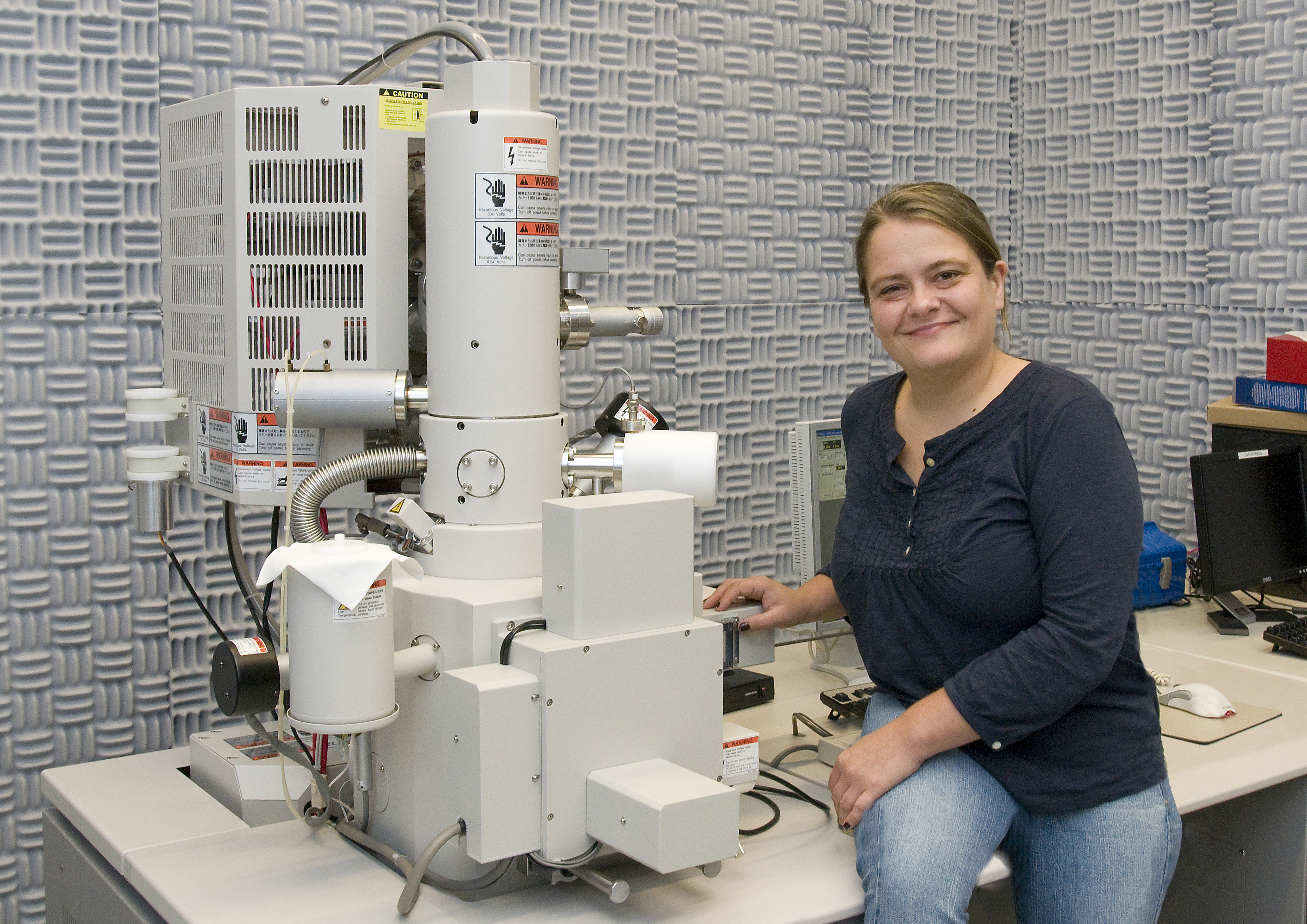
Nathalie Bouet, who leads Brookhaven's fabrication of multilayer Laue lenses, uses scanning electron microscopy at the Center for Functional Nanomaterials to image the multilayer after it has been grown. She measures the exact positioning of the layers, making sure these measurements match those expected from her team's theoretical multilayer design. This quality check is needed before the multilayer can be transformed into usable optics for the microscope.
At the U.S. Department of Energy’s (DOE) Brookhaven National Laboratory, nanofabrication—making structures or devices as small as a few atoms in size—is a daily occurrence at the Center for Functional Nanomaterials, a DOE Office of Science User Facility. Scientists at the National Synchrotron Light Source II (NSLS-II), another DOE Office of Science User Facility at Brookhaven, have been using CFN facilities to develop advanced x-ray focusing optics called multilayer Laue lenses (MLL). These optics have been incorporated into an x-ray scanning microscope installed at the Hard X-ray Nanoprobe (HXN) beamline, where they focus the extremely bright beams of “hard” (high energy) x-rays produced by NSLS-II to nanometer dimensions. Recently, this MLL-based microscope—the only one of its kind—was recognized with one of ten 2016 Microscopy Today Innovation Awards and was named a 2016 finalist for the R&D 100 Awards, which annually celebrate the world’s 100 most innovative technologies.
“These honors recognize the full extent of the development and construction of the microscope, including all of the research and development work on MLL we’ve done at the CFN,” said NSLS-II physicist Nathalie Bouet, who is leading MLL fabrication at Brookhaven.
 enlarge
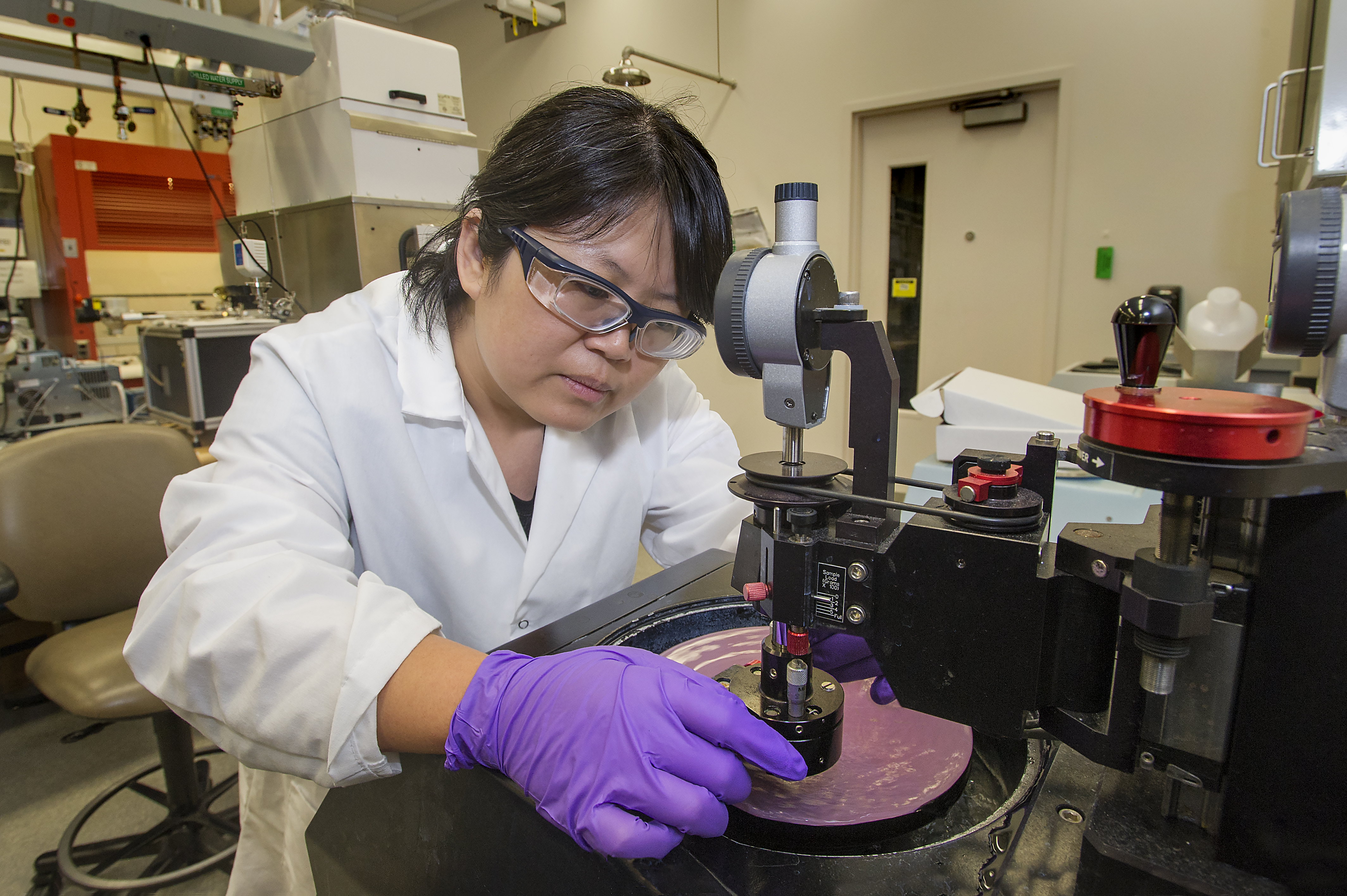
Inside the transmission electron microscopy sample preparation room at the Center for Functional Nanomaterials, Juan Zhou uses a polishing system to prepare a multilayer Laue lens.
To achieve scientific imaging with extremely high spatial resolution, the optics are integrated onto a custom-built microscope with fine motors that allow extremely accurate positioning, active feedback controls that provide vibrational stability, and components that minimize thermal drifts. With this hardware, the microscope has a resolution equivalent to 50,000 times smaller than a grain of sand. Scientists at NSLS-II use the microscope to collect elemental, structural, and chemical information on everything from soil samples to biological proteins and battery materials.
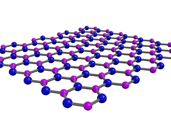
Named after physicist Max von Laue, who won the 1914 Nobel Prize in physics for his discovery of x-ray diffraction by crystals, the lenses are made up of several thousand alternating layers of two materials: silicon and tungsten silicide. To grow MLL, the scientists use a deposition system at NSLS-II that individually deposits each layer onto a silicon substrate. Layers are deposited according to a precisely controlled thickness gradient, with the thinnest layers (a few nanometers) laid first and the thickest ones (up to 25 nanometers) last.
Because even the slightest error in the multilayer stack can have a significant impact on the properties of the optics and thus, the focusing of the x-ray beam, the scientists need to analyze carefully the quality of the stack after it has been grown. Using high-resolution scanning electron microscopy at the CFN, they image the multilayer to measure the exact positioning of the layers. They compare their measurements to those expected from the theoretical multilayer design, applying this information to correct any deviations.
 enlarge
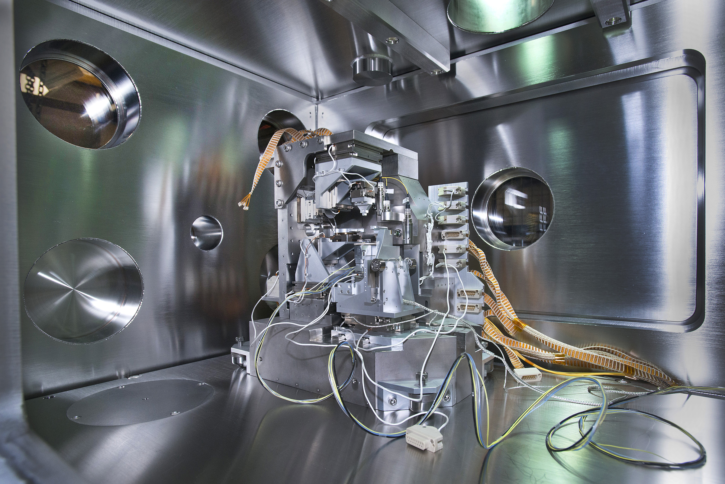
The multilayer Laue lens module is part of the x-ray microscope (seen above in a vacuum chamber) installed at the National Synchrotron Light Source II's Hard X-ray Nanoprobe beamline.
Once the multilayer stack passes the quality test, the next step is to transform it into usable optics for the microscope. To convert the multilayer stack into optics that can be illuminated in transmission, scientists precisely extract very thin sections of the stack—a very challenging endeavor.
“Sectioning is difficult because the width of the slices is significantly smaller than the thickness of the stacked layers sitting on top of the substrate,” said Brookhaven scientist Juan Zhou, a member of Bouet’s team. As a result, the multilayer sections are very susceptible to bending. If the sections contain any deformations, the lenses cannot effectively focus the x-ray beam. Therefore, very precise sectioning is crucial to ensuring that the lenses can bring x-rays into optimal focus.
 enlarge
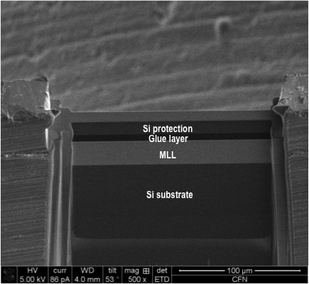
Scientists used mechanical polishing and focused-ion beam milling to fabricate the multilayer Laue lens (MLL) seen in the above scanning electron microscope image. They glued a piece of silicon (Si) on top of the multilayer film to protect it from being damaged during the lens fabrication process.
At the CFN, scientists use one of two sectioning techniques, depending on the intrinsic characteristics of the multilayer, the energy of the x-rays that will be used, and the focal length of the lens (the distance between the lens and its focal point, where the x-rays converge). The first technique is based on mechanical polishing, in which both sides of the multilayer are “gritted” down with progressively finer abrasives until the desired thickness and smoothness of the sections are achieved. The second, developed at Brookhaven, is a patented technique based on reactive-ion etching—the removal or “etching” away of a material from its surface through bombardment with a plasma of chemically reactive ions. With both techniques, the scientists often use a focused-ion beam as a final polishing tool.
Because the lenses are one-dimensional focusing optics, a pair of them is needed to make a focused beam in both directions. As a result, the spacing between the two lenses and the quality of their alignment impact the size of the x-ray beam.
 enlarge
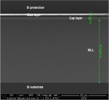
This scanning electron microscope image shows the cross-section of a multilayer Laue lens (MLL) with a thickness of 43 micrometers. The cap layer (2 micrometers thick) gives the multilayer additional protection—beyond the protection offered by the glued silicon (Si) layer—against fabrication damages.
So far, Bouet’s team has succeeded in focusing x-rays down to 11 nanometers with MLL. But efforts are underway to push the focusing even further and to maximize the number of photons in the focused beam so that HXN users can take full advantage of NSLS-II’s brightness. The team is developing MLL with a “wedged” shape, in which the layers are tilted so that their thickness differs at both ends of the substrate. (The “flat” lenses of the microscope currently in use at the HXN beamline are of equal thickness on both sides of the substrate.) Introducing a gradient inside the multilayer means each layer forms a slightly different angle than the one before it. This geometry allows MLL to diffract x-rays more efficiently; early tests have demonstrated that the wedged lenses make use of 27 percent of the x-ray beam, twice the amount used by a flat MLL.
The other members of the microscope development team are Brookhaven physicists Yong Chu (HXN beamline group leader), Xiaojing Huang, Evgeny Nazaretski, and Hanfei Yan, design engineer Brian Mullany, technical specialist Dennis Kuhne, software analyst Kenneth Lauer, as well as DOE Argonne National Lab engineer Deming Shu.
Brookhaven National Laboratory is supported by the Office of Science of the U.S. Department of Energy. The Office of Science is the single largest supporter of basic research in the physical sciences in the United States, and is working to address some of the most pressing challenges of our time. For more information, please visit science.energy.gov.
2016-6533 | INT/EXT | Newsroom