3D Nanoscale Imaging of Defects in a Nanowire
Scientists observed the formation of two kinds of defects in individual nanowires
January 31, 2018
 enlarge
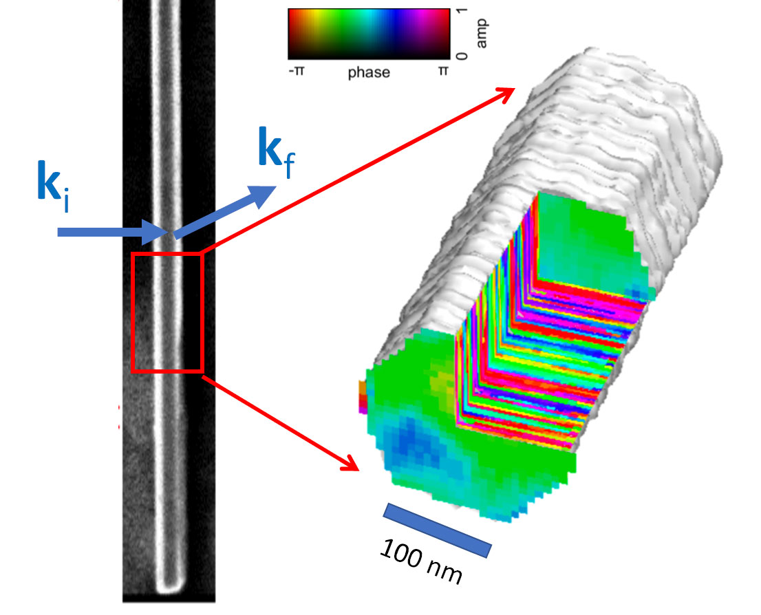
Multi-angle Bragg projection ptychography, in combination with coarse scanning measurements, enabled scientists to investigate the structure of a nanowire over three decades of length scale. The left side of the image shows an SEM scan of a nanowire with diffraction geometry, while the right shows cutouts from 3-D images sensitive to stacking defects. Image credit: Nano Letters 18(2),811-819 (2018)
The Science
In a single nanowire, the 3-D distribution of strain and stacking defects was measured using coherent x-rays, revealing structural heterogeneity from nano- to micrometer scales.
The Impact
Structural features that determine the performance of advanced optoelectronic nanodevices can be imaged by a new coherent x-ray Bragg ptychography method suitable for studies in operando.
Summary
Scientists have made many advances in nanotechnology over the last decades, which could lead to a wide range of new technologies; however, to fully understand the potential of materials such as optoelectronic nanowires, scientists need to be able see the structure of the wires at the nanoscale.
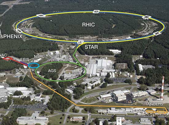
In this work, scientists used the coherent Hard X-ray Nanoprobe (HXN) beamline to investigate a single InGaAs nanowire that exhibited a number of interesting structural features spanning three decades of length scale. The HXN beamline is part of the microscopy and imaging capability suite at the National Synchrotron Light Source II (NSLS-II), a U.S. Department of Energy (DOE) Office of Science User Facility located at DOE’s Brookhaven National Laboratory.
The team of scientists analyzed nanodiffraction patterns to map lattice twists and bends across the entire nanowire length and imaged the 3-D strain at higher resolution in selected volumes via an adaptation of 3-D Bragg ptychography. This method images lattice variations by numerically inverting coherent diffraction intensity patterns.
Finally, by accessing a second Bragg peak, the scientists visualized stacking defects 3-D in the same nanowire with a resolution better than three nanometers. This image of stacking order in a nanowire is the first of its kind in the field of coherent diffraction imaging, representing a significant advance over prior work. Furthermore, this work addresses a critical gap in three-dimensional characterization of complex III-V nanowires that are a compelling route to a host of advanced electronic/opto-electronic applications.
Download the research summary slide
Related Links
Feature story: “Scientists Have a New Way to Gauge the Growth of Nanowires”
Contact
Lincoln J. Lauhon
Northwestern University
lauhon@northwestern.edu
Stephan O. Hruszkewycz
Argonne National Laboratory
shrus@anl.gov
Publication
M.O. Hill, I. Calvo-Almazan, M. Allain, M.V. Holt, A. Ulvestad, J. Treu, G. Koblmüller, C. Huang, X. Huang, H. Yan, E. Nazaretski, Y.S. Chu, G.B. Stephenson, V. Chamard, L.J. Lauhon, S.O. Hruszkewycz. Measuring Three-Dimensional Strain and Structural Defects in a Single InGaAs Nanowire Using Coherent X-ray Multiangle Bragg Projection Ptychography. Nano Letters 18(2), 811-819 (2018). DOI: 10.1021/acs.nanolett.7b04024
Funding
Development of maBPP phase retrieval and synchrotron measurements were supported by the U.S. Department of Energy (DOE), Office of Basic Energy Sciences (BES), Materials Science and Engineering Division. maBPP modeling, phase retrieval of experimental InGaAs data, and SEM characterization was supported by NSF DMR-1611341, acknowledged by L.J.L. and M.O.H. M.O.H. also acknowledges tuition and salary support of the NSF GRFP. V.C. and M.A. acknowledge funding from the European Research Council (ERC) under the European Union's Horizon H2020 research and innovation program grant agreement No 724881. M.V.H. acknowledges support from the Center for Nanoscale Materials, a U.S. Department of Energy Office of Science User Facility supported by the U.S. Department of Energy, Office of Science, under Contract No. DE-AC02-06CH11357.G.K. acknowledges financial support by the German Research Foundation (DFG), the Nanosystems Initiative Munich (NIM), and the Technical University of Munich, Institute for Advanced Study. This work made use of the EPIC facility of Northwestern University’s NUANCE Center, which has received support from the Soft and Hybrid Nanotechnology Experimental (SHyNE) Resource (NSF ECCS-1542205); the MRSEC program (NSF DMR-1121262) at the Materials Research Center; the International Institute for Nanotechnology (IIN); the Keck Foundation; and the State of Illinois, through the IIN. This research used the Hard X-ray Nanoprobe (HXN) Beamline at 3-ID of the National Synchrotron Light Source II, a U.S. Department of Energy (DOE) Office of Science User Facility operated for the DOE Office of Science by Brookhaven National Laboratory under Contract No. DE-SC0012704.
2018-17473 | INT/EXT | Newsroom