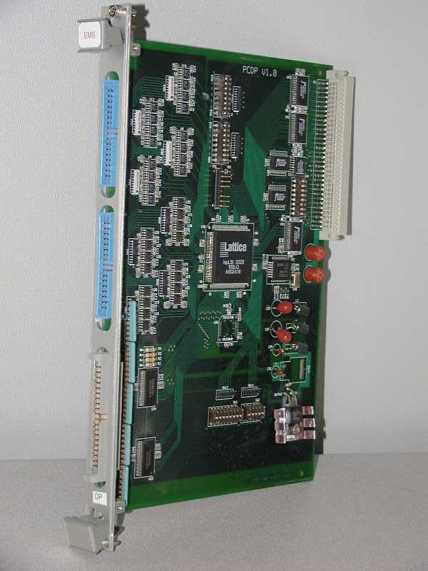
Generic PCDP module
All synchronization and most of the trigger logic on PHOBOS is built using universal programmable logic module – PCDP (Programmable Control and Data Ports). This is a custom designed A24D16 VME board (Photo) with front-panel access for 16 differential ECL (dECL) inputs and outputs, and a 17-bit differential TTL bi-directional port (dTTL). It also has a 128 KB FIFO buffer for data transfer and VME interrupt logic. The core of the module is the in-system programmable logic array ispLSI3320 [12], which can be reprogrammed in situ.
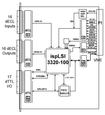
Fig 1. Block diagram of the PCDP module
The module has 20 ns propagation time from dECL inputs to dECL outputs, and is used to generate first- and second- level triggers, fast clear signals and to scale down input triggers. It is planned to use this module as a fast vertex finder. The dTTL port is used for event synchronization, alarm control and for data transfer. There are 6 PCDP modules in the system. One of them works as the event manager master (EMM), which contains the global event counter. The EMM writes the 8 least significant bits of the counter over dTTL port to dTTL ports of slave PCDP modules in other crates to signal that the new event has been accepted. The slave modules initiate the data taking process in their crates and send a handshaking signal back over a dECL line to EMM when they are ready to accept new events. After receiving the handshake from all slaves, the EMM unblocks the system.
Documentation for PHOBOS logic modules.
- PowerPoint file with L0 and L1 logic
- TML0. L0 Trigger Manager, located in the DAQ crate. Logic diagram, Signals on the front panel, ispLSI design
- TML1. L1 Trigger Manager, located in the DAQ crate. Logic diagram, Signals on the front panel, ispLSI design
- EMM. Event Manager Master, located in the DAQ crate. Signals on the front panel, ispLSI design
- EMS. Event Manager Slave, located in FASTBUS crate. ispLSI design