Segmented silicon detectors are now widely used in
spectrometers for high energy and heavy ion physics. They range
in form from the vertex locators for very large experiments at
collider accelerators, to the less complex multiplicity detectors
used in smaller, fixed target experiments. These detectors
typically contain thousands of wideband channels and must operate
under quite severe constraints in terms of mass, space and power
dissipation. Their design presents a serious challenge in
microelectronics packaging.
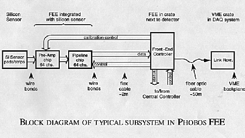
The development of the electronics for WA98 and PHOBOS is a
beautiful example of collaboration between physicists and
engineers within LNS. The front-end electronics for the PHOBOS
detector contains 120,000 channels, most of which serve the two
spectrometer arms of the detector. To maximize signal-to-noise
and to minimize the amount of cabling between the silicon
detector elements and the front-end electronics, a substantial
fraction of the electronics is mounted directly adjacent to the
silicon sensors. This portion of the electronics is configured
using a two-chip set consisting of a 64-channel preamplifier chip
and a 64-channel pipeline chip. The preamplifier chip contains a
charge-sensitive amplifier (CSA), followed by a x3 gain stage and
an output buffer. The pipeline chip contains a 16-deep
switched-capacitor analog memory followed by a dual-range 7-bit
ADC, zero-suppression logic, readout multiplexer and bus driver.
A relatively small amount of cabling connects these chips to
front-end controllers which reside in a nearby crate. The output
data from the front-end chips are stored temporarily in first-in
first-out memory in the front-end controllers, and from there the
data are transmitted via fiber-optic cable to the data
acquisition system located 150m from the detector.
The preamplifier chip was designed by collaborators at Oak Ridge
National Laboratory and MIT, and the pipeline chip was designed
by East Coast Labs, Salem, NH and MIT.
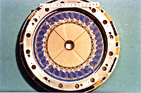
Silicon detector -- Photo courtesy of Peter Berges