Introduction       Back to contents
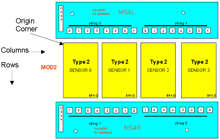
 

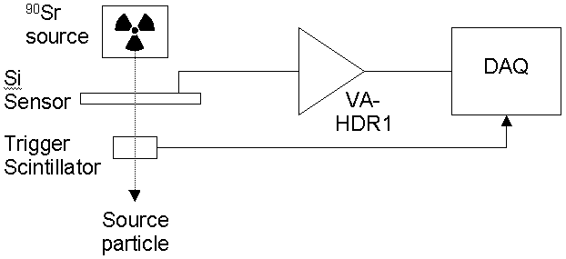
Calibration and Source Test       Back to contents

  • Why calibration?
    • Testing, immediately repairing bad bond wires etc. before any further assembly step
    • Obtaining gain (calibration) of every single channel (spectrometer including spares: 68k)
    • Find defect and noisy channels


  • Why source test?
    • Final module test, similar to beam operation
    • Study module properties
    • Determine signal and signal-to-noise

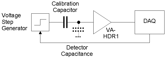
Calibration Details       Back to contents

  • Step pulse over capacitor
    • D Q = C D V
    • Ex.: 1 mV on 2 pF gives 12500 e-
    • Design considerations to minimize noise


  • Output parameter: Channel gain [mV/fC]


  • Calibration test setup
    • Hybrid/Module
    • Adapter board with step DAC and pulse generator board (E. Griesmayer, H. Frais-Kölbl), range 0..350 fC, diff. lin. better than 1%
    • CERN Repeater cards (A. Rudge)
    • NIM sequencer logic
    • National Instruments ADC board
    • PC running LabView


  • Calibration components
    • 1 capacitor is located close to each VA chip on the hybrids
    • Switching logic is integrated in the VA chips


  • Gain Uniformity
    • Within 1 chip: <3% pp

    • Chip-to-chip: <15% pp


  • Calibration allows to indentify
    • good channels
    • pinholes
    • channel shorts


  • Calibration modes
    • "Standard": done on every hybrid and module, running for about 6 months
    • "Precision": done on selected modules, special effort on stability and parameter settings, done for module properties measurements (running for a few days)


  • Calibration repeatability
    • Standard: <3% (no effort to maintain voltages like FEC)
    • Precision: <1% (as expected with FEC)


  • No charge loss due to detector capacitance
    • Could be calculated from calibrations of hybrid (w/o sensor) and module (w/ sensor) to see large effects >10%
    • Detector capacitance: 25 pF (typ.)
    • VA input capacitance: not measured
    • Charge loss below standard mode error
      ® VA input C >> detector C


  • Sample gain map for MOD20001


  • Comparison of average chip signals without and with channel calibration


Module Studies       Back to contents

  • Levels of study
    • Single sensor level
    • Single module level
    • Module/sensor comparison level


  • Typical example: MOD20001
    • 4 sensors (thicknesses 308..310 mm)
    • 5 rows, 400 columns


  • Sensor level
    • Sensor signal distribution (norm. to 300mm)

    • Fit function: Landau (3 parameters: Width, MP, Area) convoluted with Gaussian (1 parameter: Sigma)


    • Gaussian sigma represents electronic noise and intrinsic detector fluctuations (P. Shulek et al., Sov. J. Nucl. Phys. 4, 400 (1967)), typically about 2x electronic noise
    • Peak of convolute is slightly shifted from pure Landau peak (MP)


    • Sensor RMS noise map

    • Sensor MP signal vs. row


  • Module level
    • Signal and SNR distributions (norm. to 300mm)

MP = 21523 e- = 77.9 keV

SNR = 16.4


    • Relative MP signal vs. row

        Uniformity better than 1% pp !!!


Signal       Back to contents

  • Absolute MP signal vs. sensor type (normalized to 300 mm thickness)

    • Acquired with 90Sr b source
    • Average source signal: 21081 e-
    • Signal range: 20119..21552 e-
    • Signal MP agrees with capacitive loss calculation (charge sharing between detector and VA input capacities)


  • Relative MP signal vs. row

    • Uniformity: <1%
    • Very uniform even though readout lines vary in length (3..65 mm)


  • Mystery

    • 3% (1% at testbeam) difference between front and back half of hybrids
    • Intrinsic module property, reason: ?
    • We can exclude external effects because:
    • Calibration and source tests are done with the same set of repeater boards
    • Switching the ADC channels does not change anything
    • Same (though smaller) effect in testbeam with totally different DAQ hard- and software


Noise       Back to contents

      Single channel physical connections

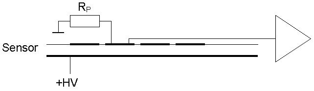
      Single channel preamp noise model
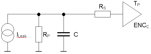
symbol

represents

typ. value

ILeak

Fraction of sensor leakage current

5 nA

RP

Parallel resistance (polysilicon)

2 MW

C

Capacitance of pad against backplane, between pads and between metal 1 and metal 2 layers

25 pF

RS

Effective serial trace resistance

40 W

TP

Shaper peaking time

1.2 ms

ENCC

Preamp noise (k + C · d)

950+5/pF e-


  • Total preamp equivalent noise charge

    • Contributions

    with ENC [e-], k [e-], d [e-/pF],
    ILeak [nA], TP [
    ms], RP [MW], RS [W]


  • Preamp noise with typical values (as stated above)

ENCC =

1078

e-

ENCILeak =

249

e-

ENCRP =

562

e-

ENCRS =

60

e-

ENC =

1243

e-


  • Shaper/Buffer and readout noise adds to preamp noise
    • Estimated shaper/buffer noise: 100 e-
    • Measured test setup readout noise: 450 e-


  • Calculated and measured noise vs. sensor type

    • Calculation and measurement agree very well
    • Measured RMS noise:
    • Average noise: 1383 e-
    • Noise range: 1230..1517 e-


Signal-to-Noise       Back to contents

  • SNR vs. Sensor Type (normalized to 300 mm)

    • Measured SNR:
    • Average SNR: 15.2
    • SNR range: 14.4..16.9


Summary       Back to contents

  • Stable calibration and source test setups
    • Gain of every single channel written into assembly database
    • Gain uniformity:
      <3% pp within chip, <15% pp chip-to-chip
    • Calibration repeatability during tests
      <1% precision


  • Gain before and after sensor mounting is the same within error bars
    • No significant charge loss by detector capacitance
    • Due to large VA input capacitance


  • Mystery
    • 3% signal difference between hybrid halves


  • "The general picture"
    • Landau-Gaussian convolute fit function
    • Typ. values (MOD20001):
    • MP signal (90Sr source) = 21500 e-
    • RMS noise = 1347 e-
    • SNR = 16.0


The sensor properties:

  • Signal (normalized to 300 mm thickness)
    • Average MP signal: 21081 e-
    • Signal range: 20119..21552 e-
      (depending on sensor type)
    • Uniformity: Signal vs. row <1% on all sensor types ® very uniform!!!


  • Noise
    • Primarily depends on detector capacitance
    • Average RMS noise: 1383 e-
    • Noise range: 1230..1517 e-
      (depending on sensor type)
    • Agrees very well with model


  • Signal-to-noise (normalized to 300 mm thickness)
    • Average SNR: 15.2
    • SNR range: 14.4..16.9
      (depending on sensor type)