New Lens Into Atomic Structures of Ultra-Thin Films
July 28, 2025
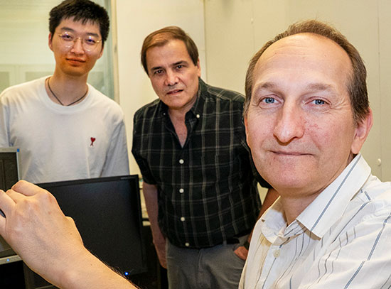
Editor’s note: The following article was originally issued by the University of Florida (UF). Daniel Olds, a beamline scientist at the Pair Distribution Function Beamline (PDF) at the National Synchrotron Light Source II — a U.S. Department of Energy Office of Science user facility at DOE’s Brookhaven National Laboratory — collaborated with scientists at UF to develop a new data processing method, IsoDAT2D, using machine learning to isolate X-ray scattering signals from thin films grown on single-crystal substrates. This work provides a deeper structural analysis of these films, helping to uncover structure–property relationships critical for future technologies, like microelectronics. For more information on Brookhaven’s role in this research, contact Denise Yazak (dyazak@bnl.gov, 631-344-6371).
By Paris Carter
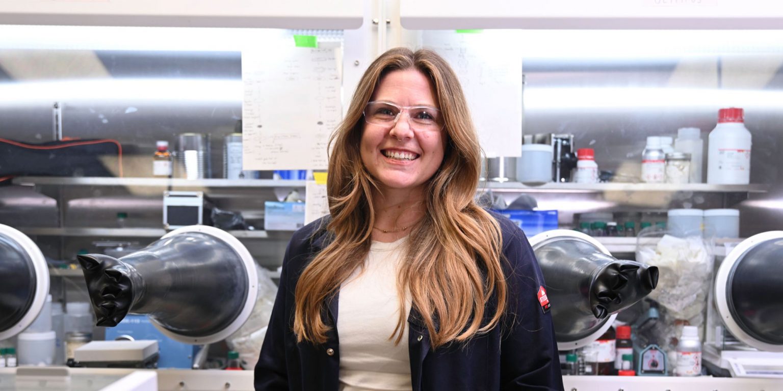
Imagine having a super-powered lens that uncovers hidden secrets of ultra-thin materials used in our gadgets. Research led by University of Florida engineering professor Megan Butala enables a novel way to look at the atomic structure of thin films on single-crystal substrates.
This research has the potential to significantly advance the development of next-generation semiconductor devices, from faster smartphones to more energy-efficient computers and powerful wearable tech. Semiconductors designed with atomic-level precision can lead to smarter, faster, more compact, and sustainable electronics.
Butala, assistant professor in the Department of Materials Science & Engineering (MSE), has developed IsoDAT2D, a machine-learning workflow for processing complex 2D X-ray total scattering data from thin film materials.
IsoDAT2D isolates and identifies the unique “fingerprints” of ultra-thin films, which are at the heart of everyday technologies we rely on. For example, computer chips are built of layers of thin films of materials, such as silicon dioxide and metal nitrides. These films are typically thousands of times thinner than human hair.
“If we understand what the atomic structure is, how to get that structure, and what properties that structure gives us, then we can design better materials from the start,” said Butala.
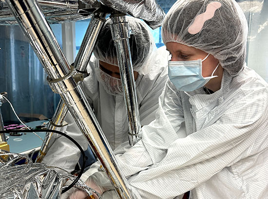
Traditionally, studying thin films on single-crystal surfaces has been difficult. Often, the atomic structure information is drawn out by larger signals from the relatively thick substrate beneath it. This large difference in the thicknesses and X-ray scattering signals makes it difficult to determine the film’s atomic structure.
Butala’s new approach improves how scientists detect extremely subtle details in a material’s atomic structure by overcoming signal-to-noise limitations in X-ray total scattering data from thin films. This capability is crucial to understanding how materials behave at the atomic level.
“This could accelerate the development of thin film materials in application environments for energy storage, semiconductors, and electronic materials, which could enable faster materials design and improve reproducibility and accessibility of X-ray scattering data,” said Butala.
MSE Interim Chair Professor Michael Tonks said Butala’s research can lead to developments that have a significant impact on the semiconductor industry and revolutionize chip manufacturing. With clearer insights, researchers can design materials with more precise properties – for example, faster and more energy-efficient computer chips.
“By developing a cutting-edge data processing tool, Dr. Butala has paved the way for researchers to study a wider range of thin films, which could lead to breakthroughs in fields ranging from energy to electronics,” said Tonks.
This could contribute to more powerful and efficient smartphones and computers, better sensors for medical devices like heart monitors and imaging tools, safer and smarter battery technologies, including e-bikes and electric cars, advanced chips for artificial intelligence, and components for quantum computers.
While the research shows promise, there are significant challenges and limitations when attempting to retrieve atomic information from thin film materials. Accurate structural analysis of thin films using IsoDAT2D requires high-quality, well-sampled input data and algorithms. Lead student researcher, recent Ph.D. MSE graduate Danielle Alverson, said developing the modular data process program was a lot of trial and error, but the journey has been quite worthwhile.
“The direction we chose, I really hope sparks other new directions. We’re combining these two machine learning algorithms, and it’s been doing OK for us. It sparks discussions at conferences and meetings. It really brings together a lot of people with the same hope of trying to understand these types of materials with these single-crystal substrates,” said Alverson.
Butala said the research would not be possible without access to the National Synchrotron Light Source-II at Brookhaven National Laboratory and a collaborator there, staff scientist Daniel Olds, Ph.D. This collaboration was essential to managing data collection challenges and developing their machine learning data processing approach.
She currently has a proposal under review at the Department of Energy and is actively pursuing other funding and collaborations with industry partners and federal agencies.
“We’re pushing the boundaries of what you can measure. We’re helping to illustrate – here are some machine learning algorithms, here’s how they can be combined in different ways. That’s part of the innovation – the combination of data preprocessing, machine learning algorithms, and post-processing,” said Butala.
The research also fits in with the United States’ quest to be a leader in developing next-generation electronics, including high-capacity advanced chips for AI applications with improved performance and lower energy consumption.
By offering researchers a clearer view of the tiniest components, it allows for more targeted design and fabrication of materials that could redefine how we interact with technology in the future.
For more details, see the published research paper:
Distinguishing isotropic and anisotropic signals for X-ray total scattering using machine learning
2025-22556 | INT/EXT | Newsroom