Toward Tinier Transistors
July 2, 2013
The foundation of many, many modern electronic devices – including computers, smart phones, and televisions – is the silicon transistor. However, the shrinking of consumer electronics is driving researchers to investigate materials that can yield thinner transistors. At NSLS, researchers have used x-rays to probe the electronic behavior of a germanium-based transistor structure, yielding important information that will guide future studies of how to make transistors smaller.
A transistor is essentially a switch that regulates the flow of current. When a certain threshold voltage is applied across it, current flows; below that, current does not flow. One very common transistor consists of a very thin (nanometer-scale) layer of an oxide (typically silicon oxide, SiO2) between a silicon substrate and a metal electrode.

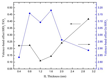
Introducing an interlayer of hafnium oxide reduces electron leakage between layers of germanium and titanium oxide, which can improve power efficiency and reliability
Germanium (Ge) is favored to replace silicon in part because charge carriers move much faster within it than in silicon (Si). But the bigger issue is the oxide layer: When SiO2 approaches a thickness of one nanometer, electrons start to “leak” through it (a result of the strange physics phenomenon of quantum mechanical tunneling), leading to excess power consumption and poor reliability. Transistors that use SiO2 cannot keep up with consumer demand for sleeker, faster devices.
Recently, companies like Intel have been making their transistors using hafnium oxide (HfO2), which can be thinner and still perform well. It has a higher “dielectric constant” (abbreviated K), which is the value that determines the robustness of any oxide against leakage: the higher the value of K, the lower the leakage. However, even HfO2 gets leaky when it's too thin.
Researchers are investigating oxides with higher K values, which, when combined with germanium, could yield a transistor more suited to tomorrow's electronics. But the most promising candidate, titanium oxide (TiO2), also leaked too much current when placed into test structures, or “heterojunctions,” regardless of whether the structures contained Si or Ge.
That leak was the result of a too-small “band offset.” This means that the TiO2 conduction bands were not adequately separated from the Si and Ge bands, allowing electrons to leak from the Si or Ge to the TiO2. A large band offset is essential when the layers are so thin, helping to keep electrons from moving between them. One research group (led by Christophe Detavernier at Ghent University in Belgium) has found a good solution: adding a thin intermediate “interlayer” to their heterojunctions before depositing the TiO2 layer. The interlayer has a more reasonable band offset. The NSLS study has used this development as a jumping-off point.
“This way, you get the best of both: the good band offset from the interlayer and the high dielectric constant of titanium oxide,” said NSLS scientist Abdul Rumaiz, the study's lead author. “However, with the scaling of devices to smaller sizes, the interlayer thickness needs to be less than one nanometer. Thus it is very crucial to understand the band offsets at such reduced dimensions.”
Rumaiz and colleagues from the National Institute of Standards and Technology (NIST), Ghent University, Quaid-i-Azam University (Pakistan), and the University of Delaware studied how interlayer thickness affected band offsets. Using x-rays at beamline X24A, which is run by NIST, they investigated germanium-based transistor structures containing TiO2 and a hafnium oxide (HfO2) interlayer. This work and future studies will be important in determining how thin the layers can be while still yielding a highly performing transistor.
The team created six samples with different interlayer thicknesses, from 0.4 nanometers (nm) to 3 nm, and a fixed TiO2 thickness of 2 nm. They studied the structure with hard x-ray photoelectron spectroscopy, or HAXPES, a technique that measures the electrons a material emits when exposed to a beam of high-energy (hard) x-rays. These measurements can tell scientists about the bulk electronic properties of a material and also reveal information about the interfaces between materials.
They began with a germanium wafer, which formed a very thin “native oxide” layer after exposure to oxygen. On top of the native oxide, the team added the HfO2 and then the titanium oxide (TiO2) using a technique called atomic layer deposition.
The HAXPES analysis showed that as the thickness of the interlayer increased, band offsets also increased. It revealed several other electronic and structural details, too. For example, the germanium native oxide shifted to a higher oxidation state, meaning that it lost electrons and also increased in thickness. There was no evidence that the TiO2 layer mixed with the HfO2 layer, but there was evidence that the HfO2 layer mixed with the germanium oxide layer below it, forming Hf-Ge bonds. The results indicate that researchers need to be cautious about making assumptions about band offset.
This research is published in the November 27, 2012, online edition of Applied Physics Letters.
2013-4120 | INT/EXT | Newsroom


