Structural Distortions Emerge from Nothing at the Nanoscale
Newly discovered phase helps explain materials' ability to convert waste heat to electricity
December 16, 2010
The following news release is being issued jointly by the U.S. Department of Energy's Brookhaven National Laboratory and Columbia University¹s School of Engineering and Applied Science. Columbia Engineering media contact: Holly Evarts, 212 854-3206, holly@engineering.columbia.edu.
 enlarge
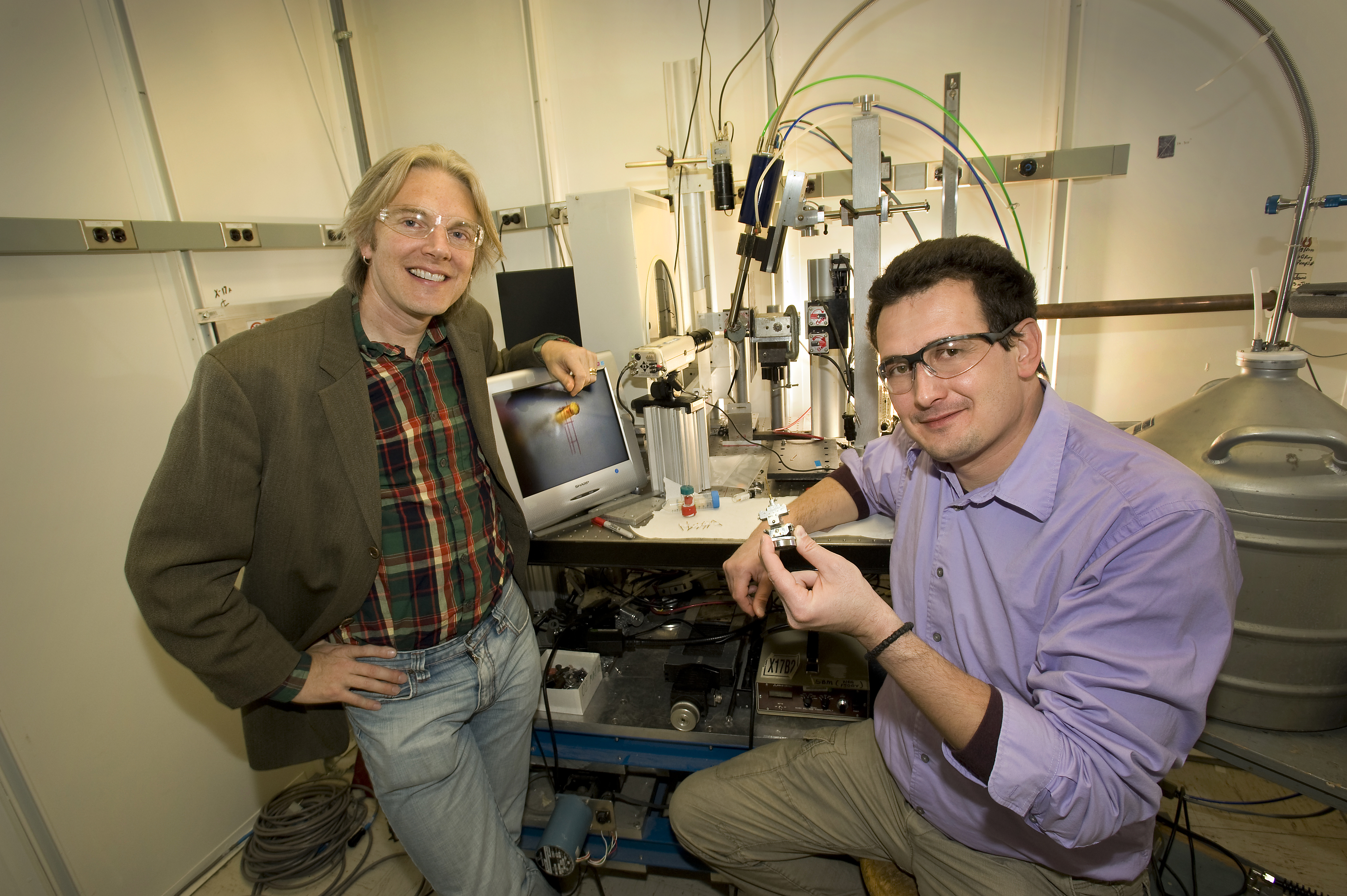
Simon Billinge (left) and Emil Bozin (right) at beamline X17A at the National Synchrotron Light Source (NSLS) at Brookhaven Lab, where the scientists will continue their explorations of local atomic structure to identify materials useful for energy applications.
Scientists have discovered that a class of materials known to convert heat to electricity and vice versa behaves quite unexpectedly at the nanoscale in response to changes in temperature. The discovery — described in the December 17, 2010, issue of Science — is a new "opposite-direction" phase transition that helps explain the strong thermoelectric response of these materials. It may also help scientists identify other useful thermoelectrics, and could further their application in capturing energy lost as heat, for example, in automotive and factory exhaust.
The scientists — from the U.S. Department of Energy's (DOE) Brookhaven National Laboratory, Columbia University, Argonne National Laboratory, Los Alamos National Laboratory, Northwestern University, and the Swiss Federal Institute of Technology — were studying lead chalcogenides (lead paired with tellurium, selenium, or sulfur) using newly available experimental techniques and theoretical approaches that allow them to "see" and model behavior of individual atoms at the nanoscale, or on the order of billionths of a meter. With those tools they were able to observe subtle changes in atomic arrangements invisible to conventional probes of structure.
To understand the phase transition the scientists observed, think of the everyday response of a gas like steam cooling to form liquid water, and then freezing to form solid ice. In each case, the atoms undergo some form of structural rearrangement, explains Simon Billinge, a physicist at Brookhaven Lab and Columbia University's School of Engineering and Applied Science and a lead author on the Science paper.
"Sometimes, further cooling will lead to further structural transitions: Atoms in the crystal rearrange or become displaced to lower the overall symmetry," Billinge says. The development of such localized atomic distortions upon cooling is normal, he says. "What we discovered in lead chalcogenides is the opposite behavior: At the very lowest temperature, there were no atomic displacements, nothing — but on warming, displacements appear!"
The techniques the scientists used to observe this nanoscale atomic action were high-tech versions of x-ray vision, aided by mathematical and computer analysis of the results. First the lead materials were made in a purified powder form at Northwestern University. Then the scientists bombarded the samples with two kinds of beams — x-rays at the Advanced Photon Source at Argonne and neutrons at the Lujan Neutron Scattering Center at Los Alamos. Detectors gather information about how these beams scatter off the sample to produce diffraction patterns that indicate positions and arrangements of the atoms. Further mathematical and computational analysis of the data using computer programs developed at Brookhaven and Columbia allowed the scientists to model and interpret what was happening at the atomic level over a range of temperatures.
Brookhaven physicist Emil Bozin, first author on the paper, was the first to notice the odd behavior in the data, and he worked tenaciously to prove it was something new and not a data artifact. "If we had just looked at the average structure, we never would have observed this effect. Our analysis of atomic pair distribution functions gives us a much more local view — the distance from one particular atom to its nearest neighbors — rather than just the average," Bozin says. The detailed analysis revealed that, as the material got warmer, these distances were changing on a tiny scale — about 0.025 nanometers — indicating that individual atoms were becoming displaced.
The scientists have made an animation to illustrate the emergence of these displacements upon heating. In it, the displacements are represented by arrows to indicate the changing orientations of the atoms as they flip back and forth, or fluctuate, like tiny dipoles.
According to the scientists, it is this random flipping behavior that is key to the materials' ability to convert heat into electricity.
"The randomly flipping dipoles impede the movement of heat through the material in much the same way that it is more difficult to move through a disorderly wood than an orderly apple orchard where the trees are lined up in rows," Billinge says. "This low thermal conductivity allows a large temperature gradient to be maintained across the sample, which is crucial to the thermoelectric properties."
When one side of the material comes in contact with heat — say, in the exhaust system of a car — the gradient will cause charge carriers in the thermoelectric material (e.g., electrons) to diffuse from the hot side to the cold side. Capturing this thermally induced electric current could put the "waste" heat to use.
This research may help scientists search for other thermoelectric materials with exceptional properties, since it links the good thermoelectric response to the existence of fluctuating dipoles.
"Our next step will be searching for new materials that show this novel phase transition, and finding other structural signatures for this behavior," Billinge said. "The new tools that allow us to probe nanoscale structures are essential to this research.
"Such studies of complex materials at the nanoscale hold the key to many of the transformative technological breakthroughs we seek to solve problems in energy, health, and the environment."
This research was funded by the DOE Office of Science, the Office of Naval Research, and the National Science Foundation.
Columbia University's Fu Foundation School of Engineering and Applied Science offers programs to both undergraduate and graduate students who undertake a course of study leading to the bachelor's, master's, or doctoral degree in engineering and applied science. With facilities specifically designed and equipped to meet the laboratory and research needs of faculty and students, Columbia Engineering is home to a broad array of basic and advanced research installations, from the Columbia Center for Electron Transport in Molecular Nanostructures to the Columbia Genome Center. These interdisciplinary centers in science and engineering, materials research, nanoscale research, and genomic research are leading the way in their respective fields while individual groups of engineers and scientists collaborate to solve some of society's more vexing challenges. www.engineering.columbia.edu.
2010-11206 | INT/EXT | Newsroom