Q&A with CFN User Davood Shahrjerdi
Combining the unique properties of emerging nanomaterials with advanced silicon-based electronics, NYU's Shahrjerdi engineers nano-bioelectronics
April 18, 2017
 enlarge
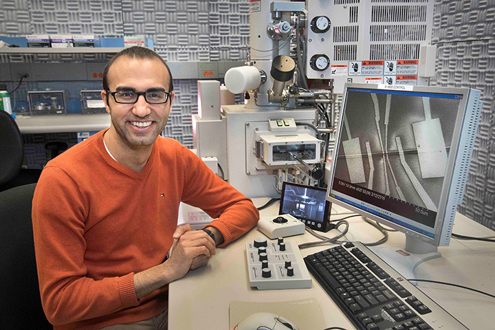
Davood Shahrjerdi in the scanning electron microscope facility at Brookhaven Lab's Center for Functional Nanomaterials (CFN). The image on the screen is a Hall bar structure for measuring carrier transport in a semiconductor wire.
Davood Shahrjerdi is an assistant professor of electrical and computer engineering at New York University (NYU) and a principal investigator at the NYU Laboratory for Nano-Engineered Hybrid Integrated Systems. Shahrjerdi, who holds a doctorate in solid-state electronics from The University of Texas at Austin, engineers nanodevices for sensing and life science applications through integrating the unique properties of emerging nanomaterials with advanced silicon-based electronics. For the past two years, he has been using facilities at the Center for Functional Nanomaterials (CFN)—a U.S. Department of Energy (DOE) Office of Science User Facility at Brookhaven National Laboratory—to fabricate and characterize these nanodevices.
What is the mission of the NYU Laboratory for Nano-Engineered Hybrid Integrated Systems?
My lab’s mission is to create new electronic devices for sensing and life science applications. To achieve this goal, we combine the benefits of emerging nanomaterials—such as two-dimensional (2D) materials like graphene—and advanced silicon integrated circuits. These nano-engineered bioelectronic systems offer new functionalities that exist in neither nanomaterials nor silicon electronics alone. At the moment, we are leveraging our expertise to engineer new tools for neuroscience applications.
We are also doing research for realizing high-performance flexible electronics for bioelectronics applications. Our approach is two pronged: (1) flexible electronics using technologically mature materials, such as silicon, that are conventionally mechanically rigid, and (2) flexible electronics using atomically thin 2D nanomaterials that are inherently flexible.
Given the resources of NYU and the plethora of nanotechnology research centers in the surrounding New York City area, why bring your research to CFN?
Before I joined academia, I was a research staff member at the IBM Thomas J. Watson Research Center, where I had easy access to advanced fabrication and characterization facilities. When I joined NYU in September 2014, I began to look for research facilities to pursue my research projects. In my search, I discovered CFN and reached out to its scientists, who were very helpful in explaining the research proposal process and the available facilities for my research. In the past two years, my research projects have evolved tremendously, and access to CFN laboratories has been instrumental to this evolution. Because research-active scientists maintain CFN labs, I can conduct my research without major hiccups—a rare occurrence in academia, where equipment downtime and process changes could set back experiments.
It is not only the state-of-the-art facilities but also the interactions with scientists that have made CFN invaluable to my research. I could use other fabrication facilities in Manhattan, but I prefer to come to CFN. At IBM, I could walk out of my office and knock on any door, gaining access to the expertise of chemists, physicists, and device engineers. This multidisciplinary environment similarly exists at CFN, and it is conducive to driving science forward. Bringing my research to the CFN also means that my doctoral students and postdocs have the opportunity to use state-of-the-art facilities and interact with world-class scientists.
What tools do you use at CFN to conduct your research, and what are some of the projects you are currently working on?
We synthesize the 2D nanomaterials at my NYU lab, with subsequent device fabrication and some advanced material characterization at CFN. After device fabrication, we perform electrical characterization at my NYU lab.
In addition to using the materials processing capabilities in CFN’s clean room, we use advanced material characterization capabilities to glean information about the properties of our materials and devices at the nanoscale. These capabilities include transmission electron microscopy (TEM) to study the structure of the materials, X-ray photoelectron spectroscopy to examine their chemical state, and nano-Auger electron spectroscopy to probe their elemental composition.
 enlarge
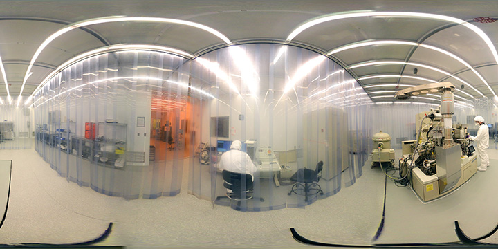
The 5,000-square-foot clean room at CFN is dedicated to state-of-the-art processing of thin-film materials and devices. Capabilities include high-resolution patterning by electron-beam and nanoimprint lithography methods, plasma-based dry etch processes, and material deposition.
One of our projects is the large-area synthesis of 2D transition metal dichalcogenide semiconductors, which are materials that have a transition metal atom (such as molybdenum or tungsten) sandwiched between two chalcogen atoms (sulfur, selenium, or tellurium). Using a modified version of chemical vapor deposition (referring to the deposition of gaseous reactants onto a substrate to form a solid), my team synthesized a monolayer of tungsten disulfide that has the highest carrier mobility reported for this material. I am now working with CFN scientists to understand the origin of this high electrical performance through low-energy electron microscopy (LEEM). Our understanding could lead to the development of next-generation flexible biomedical devices.
 enlarge
The single-atom-thick tungsten disulfide (illustration, left) can absorb and emit light, making it attractive for applications in optoelectronics, sensing, and flexible electronics. The photoemission image of the NYU logo (right) shows the monolayer material emitting light.
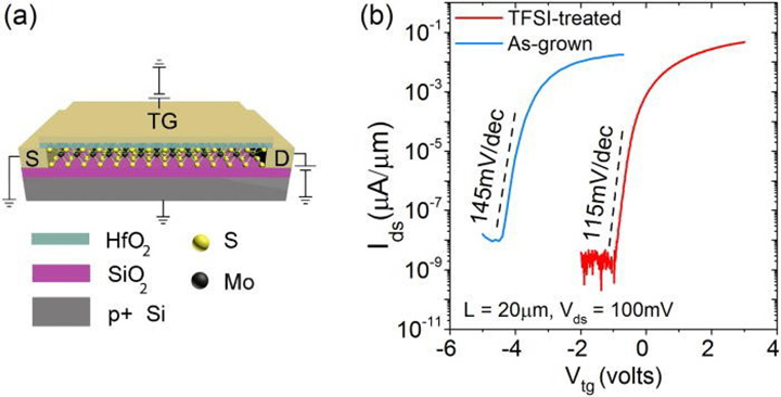
Recently, our team together with CFN scientists published a paper on studying the defects in another 2D transition metal dichalcogenide, monolayer molybdenum disulfide. We treated the material with a superacid and used the nano-Auger technique to determine which structural defects were “healed” by the superacid. Our electrical measurements revealed the superacid treatment improves the material’s performance.
 enlarge
Shahrjerdi and his team fabricated top-gated field-effect transistors (FETs)—devices that utilize a small voltage to control current—on as-grown and superacid-treated molybdenum disulfide films. A schematic of the device is shown in (a). As seen in the graph (b), the chemical treatment (TFSI, red line) improves the electronic properties of the device. From Applied Physics Letters 110, 033503 (2017).
Another ongoing project in my NYU lab involves a collaborative effort with the NYU Center for Neural Science to develop next-generation neuroprobes for understanding not only the electrical signaling in the brain but also the chemical signaling. This problem is challenging to solve, and we are excited about the prospects of nanotechnology for realizing an innovative solution to it.
In fabricating nanoelectronic materials and components, what are some of the challenges you face?
Nanomaterials are usually difficult to handle—they are often very thin and are highly sensitive to defects or misprocessing. As a result, reproducibility could be a challenge. To understand what is causing a particular observed behavior, we have to fabricate many samples and try to reproduce the same result to understand the physical origin of an observed behavior.
Also, it often happens that you expect to observe a certain behavior but you might end up observing an anomalous behavior that could lead to new discoveries. For example, I accidentally stumbled on the epitaxial growth of silicon on silicon at 120-degrees Celsius while playing around with hydrogen dilution during the deposition of amorphous silicon. This temperature is much lower than the usual temperature required by the traditional approach. My IBM collaborators and I published the work, and it actually led to a best paper award from the Journal of Electronic Materials!
What is the most exciting thing on the horizon for nanoelectronics? What do you personally hope to achieve?
Over the next 5 to 10 years, the field of nanoelectronics has great potential to transform our lives—especially in the areas of bioelectronics and bio-inspired electronics, with the marriage between nanomaterials and conventional electronics leading to new discoveries in the life sciences.
Biosensing is the area that I am most passionate about. The research community still has a limited understanding of how the brain functions, hindering the progress for developing treatments and drugs for neurological disorders such as Parkinson’s. Developing next-generation sensors that advance our understanding of the brain will have tremendous economic and societal impact. I am very excited about our neuroprobe project.
Also, better understanding of the brain could lead to new discoveries for realizing next-generation computing systems that are inspired by the brain. For example, nanoscale memory devices that could mimic the synapses of the brain would open new horizons for brain-inspired computing. I am engaged in a collaborative effort with The University of Texas at Austin to explore the prospects of nanoscale memristors (short for memory resistor, a new class of electrical circuits with memories that retain information even after the power is shut off) for such an application.
NYU is home to the second-highest number of international students in the United States, representing more than 130 different countries, and CFN employs staff and hosts users from around the world. How has being in these multicultural environments impacted your research?
I believe science has no boundaries because it is shared by people who are driven by their curiosity to discover unknowns and have the desire to better humanity. These sentiments are at the core of scientific communities. Though we may have different backgrounds, our common ground is working on problems that have not yet been solved or discovering the undiscovered.
How did you become interested in science in general and specifically neuroscience?
As a kid, I was fascinated with science, particularly physics, and building things. By high school, I had also developed an interest in biology and particularly the brain. When I completed high school in Iran, I had to make the decision of whether I wanted to pursue an undergraduate degree or attend medical school. In Iran, there are no pre-med programs—you start medical school directly after high school, and you cannot enroll in medical school after you have taken the undergraduate route.
My passion at the time was electrical engineering, so I went for the undergraduate degree. This passion evolved into device physics, my PhD field. After a few years at IBM as a device physicist, my love of bioelectronics was rekindled. I started studying neuroscience and even contemplated attending medical school in the United States. Finally, I decided to join academia and apply my knowledge of physics and electronics to the area of bioelectronics. I feel fortunate to have found a career in which I can combine my expertise and interests.
2017-12161 | INT/EXT | Newsroom


