Taking Hybrids for a Spin to Generate Electricity from Sunlight
New findings on charge transfer in nanoscale pairings of materials may lead to efficient solar cells and other applications
June 14, 2012
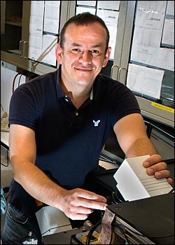
Mircea Cotlet
Even at the nanoscale, hybrids show promise — as evidenced by new efforts to pair inorganic nanoparticles with conductive polymers to convert sunlight into electricity or build better biosensors. To make the most of these molecular matchups, however, scientists need to understand the small-scale details of charge transfer — and how to control it.
Scientists working at the Center for Functional Nanomaterials (CFN) at the U.S. Department of Energy’s Brookhaven National Laboratory together with their colleagues at Syracuse University recently demonstrated this kind of precision control in a hybrid composed of light-absorbing quantum dots and a conjugated polymer — two types of semiconducting materials that have been widely studied for photovoltaic and other optoelectronic applications and biosensors. They’ve published a paper describing the details of the hybrid nanocomposite self-assembly enabling control of the charge transfer rate in the journal ACS Nano (available online June 11, 2012).
“Photovoltaic solar cells that incorporate organic and inorganic semiconducting materials could be inexpensive to manufacture,” said Brookhaven physical chemist Mircea Cotlet, who led the research team. “But we need to design them in such a way that they are easy to assemble and efficient at absorbing light and separating charges to produce electric current.”
On the other hand, scientists are also interested in using such hybrid composites to produce light emitting diodes and biosensors, where the production of such separated charges reduces the amount of light generated via the quantum dots’ photoluminescence, and is therefore detrimental. “We need to understand the details of how these materials operate under various conditions so we can optimize the properties for the desired application,” Cotlet said.
For the current study, the scientists took advantage of electrostatic attraction to get negatively charged quantum dots and a positively charged polymer to self-assemble to form hybrids, and then tested the strength of one kind of charge transfer under a variety of conditions. By illuminating the quantum dots with a particular wavelength of light, they could measure how positive charges known as “holes” were extracted in a controlled way by the nearby polymer at the expense of the photoluminescence emitted by the quantum dot.
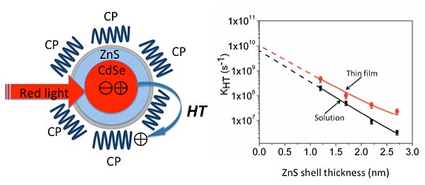
Illuminating a hybrid nanomaterial composed of a core/shell quantum dot surrounded by a conjugated polymer (CP) with red light leads to the transfer of positive charges called holes from the quantum dot to the polymer. By varying the thickness of the zinc-sulfide (ZnS) shell surrounding the cadmium-selenide (CdSe) core, scientists can control the rate of hole transfer (HT), with thinner shells increasing the transfer rate both in solution and on thin films made of the composite.
The key variable they were interested in studying was how the hole transfer rate was affected by the thickness of an optically inert shell surrounding the core of each quantum dot. To test this, the scientists at Syracuse chemically synthesized a series quantum dots with varying shell thickness, from very thin (1 nanometer) to thick (4 nm), and capped them with the conjugated polymers.
“We were really excited to design and synthesize the quantum dots needed for this study,” said Syracuse University chemist Mathew Maye, whose team regularly uses the CFN facility for its research. “There are still many unknowns in nanoscale energy transfer, and thanks to this study, we now are closer to optimizing all the fine details.”
The results clearly show that photoluminescence and charge transfer are competing processes: As the shell thickness increased, the rate of charge transfer decreased and photoluminescence increased. Conversely, thicker shells resulted in more intense photoluminescence and a lower hole transfer rate.
This implies that the shell acts as a “tunneling barrier” slowing down the flow of holes from the dot to the polymer, Cotlet said.
“If you want to design such hybrid materials for photovoltaic solar cell applications, you may want to use dots with a very thin shell or no shell at all to produce as many charges as you can,” he said. “But because such hole transfer quenches, or kills, the photoluminescence of the dot, a thicker shell may be a better option for applications like light emitting diodes or biosensors.”
The scientists found the same inverse relationship between shell thickness and charge transfer rate no matter whether the hybrid materials were in solution or thin films, but hole transfer rates were better overall in the thin film condition than in solution. “This is good news since thin films are the most likely configuration for photovoltaic devices,” Cotlet said.
Additional experiments looking at single hybrid particles also found fluctuations in the rate of charge transfer that were dependent on the dot’s shell thickness.
“These kinds of fluctuations can affect the amount of current that comes out of a device, so we’d want to find ways to stabilize this in a device.” Cotlet said. “Only by looking at single particles, as we’ve done here for the first time, can you track this kind of fluctuating behavior,” he said.
Overall, the findings show that the nanoparticle synthesis and self-assembly methods used to engineer quantum dots with various shell thicknesses can give scientists the control they need over optoelectronic properties. “Whether we want to maximize hole transfer rate for photovoltaic applications, or alternatively, photoluminescence for biosensors, we now have a way to do that,” Cotlet said.
In addition to Cotlet and Maye, Zhihua Xu (Brookhaven Lab) and Corey Hine (Syracuse U) were part of the team that performed the study.
This research was funded by the U.S. Department of Energy’s Office of Science (BES), the American Chemical Society, and the Air Force Office of Scientific Research.
The Center for Functional Nanomaterials at Brookhaven National Laboratory is one of the five DOE Nanoscale Science Research Centers (NSRCs), premier national user facilities for interdisciplinary research at the nanoscale. Together the NSRCs comprise a suite of complementary facilities that provide researchers with state-of-the-art capabilities to fabricate, process, characterize and model nanoscale materials, and constitute the largest infrastructure investment of the National Nanotechnology Initiative. The NSRCs are located at DOE’s Argonne, Brookhaven, Lawrence Berkeley, Oak Ridge and Sandia and Los Alamos national laboratories. For more information about the DOE NSRCs, please visit http://nano.energy.gov.
DOE’s Office of Science is the single largest supporter of basic research in the physical sciences in the United States, and is working to address some of the most pressing challenges of our time. For more information, please visit science.energy.gov.
Related Links
Scientific paper: “Shell Thickness Dependent Photoinduced Hole Transfer in Hybrid Conjugated Polymer/Quantum Dot Nanocomposites: From Ensemble to Single Hybrid Level”
2012-3148 | INT/EXT | Newsroom