Organic Crystal Film Grown on New Substrate Breaks Performance Record
The study is an important step toward realizing mainstream organic electronic devices
November 18, 2014
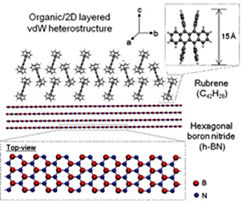
Organic two-dimensional heterostructure of rubrene/h-BN
Many future electronic devices may be based not on standard conductors and semiconductors but rather on small organic (carbon-based) molecules and polymers. These organic electronics will have several advantages over conventional electronics, including being cheaper to fabricate, physically bendable and flexible, and, in some cases, can be created using printing methods – perhaps even in your own home.
The field of organic electronics is still in its infancy, however, and scientists have much to learn before organic electronic devices are part of our everyday lives. One obstacle researchers have faced is how to successfully grow high-quality crystals of an organic molecule on top of a conventional substrate – without using a complex growth process or chemically modifying the substrate first. Solving this problem is the necessary first step to creating organic electronic circuits and devices.
Recently, a research group made some significant headway. Working in part at the National Synchrotron Light Source (NSLS), scientists from Columbia University, Harvard University, Brookhaven Lab, and Japan's National Institute for Materials Science grew a high-quality, high-performing film of rubrene, an organic semiconductor, onto a substrate of hexagonal boron nitride, a layered crystalline material with hexagonally shaped molecular units (similar to graphite carbon). Their work, which they discuss in the May 14, 2014, edition of the journal Advanced Materials, is notable both due to the high-quality crystalline nature of the film and because the substrate is a new player in the field of organic electronics development.
“The interface between the substrate and the molecular film is very important. It governs the initial nucleation during the growth of the film and also has a big impact on how the film will carry charge,” says Columbia researcher Phillip Kim, one of the paper's authors. “Our film/substrate heterostructure yielded the highest mobility observed yet in similar systems. It is comparable to those of free-standing single crystals and represents a record for organic films grown on any substrates.”
When paired with organic materials, conventional substrates like silicon oxide, glass, and plastic are too disordered at the molecular level and also don't have molecular structures that are similar enough to the organic compounds. In materials science terms, they lack an “epitaxial” relationship. This discourages proper film growth and results in lower-quality films that lack long-range order. In everyday terms, this is kind of like trying to build a layer of Lego bricks on Lego board that doesn't have an ordered grid of nubs.
Kim and his colleagues showed that hexagonal boron nitride (h-BN) has many advantages as a substrate for organic electronics. Using an approach called “van der Waals epitaxy,” a method that takes advantage of the weak van der Waals force between molecules, the group grew rubrene films varying from 5 to 1000 nanometers thick. They studied each sample's structure and charge-carrying ability using several methods.
Atomic force microscopy (AFM) and transmission electron microscopy (TEM) images suggested that the film was formed of large single-crystal domains. Selected area electron diffraction (SAED), which can be performed inside a transmission electron microscope, also confirmed this. But because SAED provides only local structural information, the group used grazing x-ray diffraction at NSLS beamline X9 to get a broader “view” of the structure. The x-ray data showed sharp, intense peaks, indicating that the sample contained a high-quality crystal structure.
To study how the film carries charge, graphene electrical contacts were incorporated into the growth process, resulting in a field-effect transistor structure. Measuring the current across it showed that electrons traveling within it are highly mobile, meaning they don't run into too many barriers caused by a “choppy” molecular structure.
“Our study highlights the advantages of h-BN and similar materials over commonly used substrates to achieve high-performance organic electronic devices,” said Kim. “More generally, this approach to film growth – van der Waals epitaxy – could be used to fabricate organic/inorganic structures that can be readily expanded to numerous other organic and layered materials for various electronic applications.”
This research was supported by: the Center for Redefining Photovoltaic Efficiency Through Molecule Scale Control, an Energy Frontier Research Center funded by the U.S. Department of Energy, Office of Science, Office of Basic Energy Sciences; the FAME Center, one of six centers of STARnet, a Semiconductor Research Corporation program sponsored by MARCO and DARPA; the Nano Material Technology Development Program through the National Research Foundation of Korea funded by the Ministry of Science, ICT and Future Planning; the Basic Science Research Program through the National Research Foundation of Korea; the U.S. Department of Energy, Office of Basic Energy Sciences, under the Extreme Science and Engineering Discovery Environment, supported by the National Science Foundation.
2014-5366 | INT/EXT | Newsroom


