Why Calcium Improves a High-Temperature Superconductor
June 7, 2004
UPTON, NY - Scientists at the U.S. Department of Energy's Brookhaven National Laboratory have found evidence to prove why adding a small amount of calcium to a common high-temperature superconductor significantly increases the amount of electric current the material can carry. This research may be a first step toward developing commercial applications for high-temperature superconducting materials. The results appear in the May 15, 2004 issue of Physical Review Letters.
 enlarge
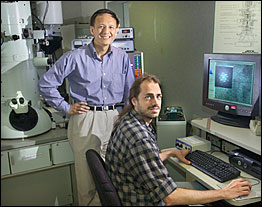
Yimei Zhu (left) and Marvin Schofield, in front of the transmission electron microscope they used to perform the research. (Click image for hi-res version.)
"Many materials classified as high-temperature superconductors exhibit good properties only in single-crystal form and are actually unsuitable for practical applications, such as high-efficiency electrical wire, because their bulk composition - individual crystalline grains - disrupts the flow of electrons," said Yimei Zhu, a Brookhaven physicist who led the research.
"But for practical applications in which large electric currents need to be transported, such as power cables, the polycrystalline forms must be used. These polycrystalline materials carry a very low current compared to their single-crystal counterparts," he said.
This is due to the problem of grain boundaries - the interfaces created between adjacent grains. At grain boundaries, incoming electrons slow down or change direction, thus losing momentum and releasing the lost energy as heat. This results in low electron flow across the boundaries - exactly the opposite of "good" superconductor behavior.
Researchers theorized that electric voltage barriers at the grain boundaries are the cause of this problem. Now, the Brookhaven scientists have found evidence to support this theory.
"We discovered why grain boundaries are the predominant factor that limits the current flow in these materials," said Brookhaven physicist Marvin Schofield, the paper's principle author.
"By understanding grain boundary behavior, we can engineer grain boundaries with improved properties. This is a major challenge in superconductor research, which may lead to the commercialization of high-temperature superconducting materials that could revolutionize our daily lives in the near future."
Scientists worldwide have studied YBCO, a high-temperature superconductor named for the elements it contains - yttrium, barium, copper, and oxygen. They know that it conducts significantly better when it is "doped" with calcium, but have not known, until now, why this is true. The Brookhaven scientists determined this by comparing calcium-doped YBCO to undoped YBCO.
The evidence lies in the areas within grain boundaries in which adjacent grains are most mismatched. To visualize this, picture a centimeter-based ruler next to an inch-based one, where the tick marks on each ruler represent the positions of atoms in the crystal structure of two adjacent, slightly different grains. The marks will match in some cases, nearly match in others, and misalign completely in the rest.
In undoped YBCO, the scientists found, the electrons encounter the most electrical resistance at the most misaligned regions, where the voltage barrier is wide and high. Doping YBCO with calcium causes these regions to shrink, both in width and height. As a result, Schofield and his colleagues determined that calcium doping increases the current across the grain boundary by 35 percent.
To perform the research, the Brookhaven scientists used a YBCO "bicrystal," a type of crystal grown to contain just one grain boundary, much like two very large grains merged together. The electromagnetic properties of bicrystals are well characterized, allowing the researchers to pinpoint what happens to the electrons at the boundary upon calcium doping, using the results as a model for the overall material. Bicrystals eliminate the impossible task of isolating one boundary out of thousands in the material sample.
To closely examine the bicrystal grain boundary, the scientists used a transmission electron microscope (TEM), a device that uses electrons as tiny probes to "see" inside materials. A sample is placed inside the TEM and bombarded with electrons. As the electrons pass through the sample, they are scattered away from the charged regions of the material. When they emerge, they carry information about the electric and magnetic fields within the sample. This information is then retrieved by a method known as electron holography.
"With electron holography," Schofield explained, "we can see exactly what the electrons in the material see at the grain boundary. Thus, this method takes us a tremendous step closer to understanding the role grain boundaries play in the properties of real materials."
Additional collaborators instrumental in this research were Marco Beleggia, of Brookhaven Lab, and Karsten Guth and Christian Jooss, both of the University of Gottingen in Germany. The work was funded by the Office of Basic Energy Sciences within the U.S. Department of Energy's Office of Science and the German Research Foundation.
2004-10189 | INT/EXT | Newsroom


