Electronics Play By a New Set of Rules at the Molecular Scale
September 2, 2012
By Aviva Hope Rutkin
 enlarge
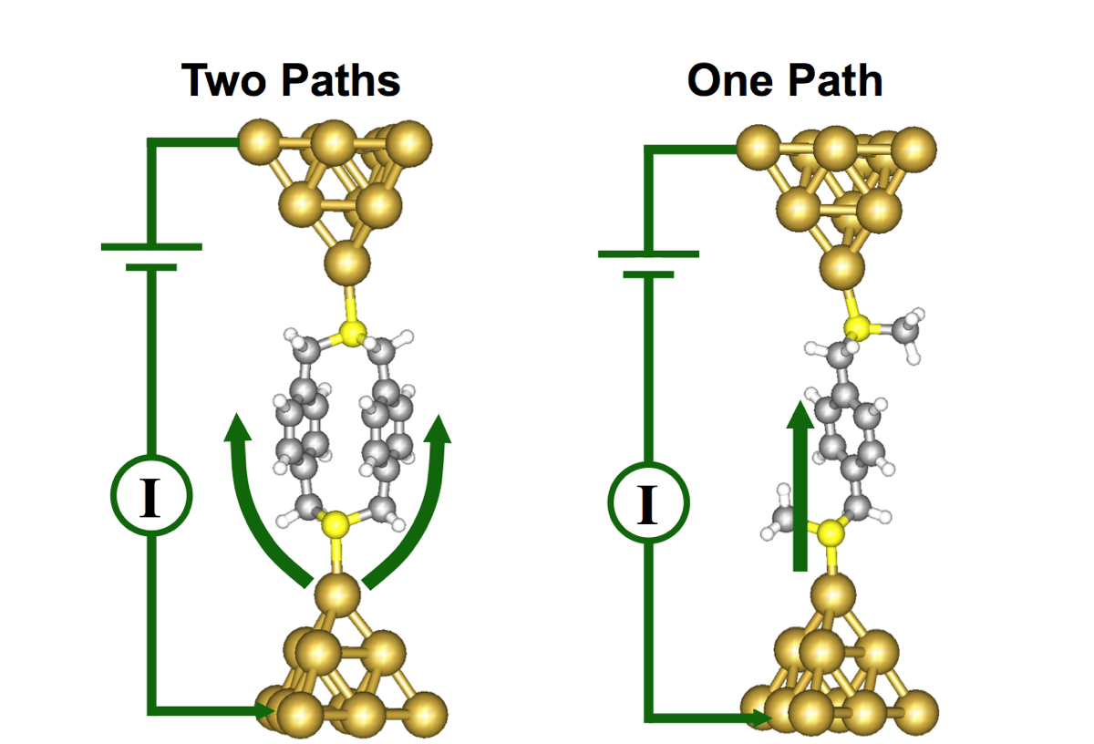
Atomic scale visualization of the single molecule junctions formed with two equivalent pathways (left) and one pathway (right), including the bonding to the tips of two gold electrodes and a schematic of the external electrical circuit.
In a paper published in Nature Nanontechnology on September 2, 2012, scientists from the U.S. Department of Energy’s (DOE) Brookhaven National Laboratory and Columbia University’s departments of Chemistry and of Applied Physics explore the laws that govern electronic conductance in molecular scale circuits.
“Everyone who has worked with basic electronic circuits knows that there are some simple rules of the road, like Ohm’s Law,” explains collaborator Mark Hybertsen, a physicist at Brookhaven’s Center for Functional Nanomaterials (CFN). Hybertsen provided the theory to model the observed circuit behavior with the CFN’s computational tools. “For several years we have been asking fundamental questions to probe how those rules might be different if the electronic circuit is shrunk down to the scale of a single molecule.”
Conductance measures the degree to which a circuit conducts electricity. In a simple circuit, if you hook the resistors up in parallel, the electrons can flow through two different paths. In this case, the conductance of the full circuit will simply be the sum of the conductance of each resistor.
However, in a molecular circuit, the rules that govern current flow now involve fundamental quantum mechanics. In most single-molecule circuits, the molecules do not behave like conventional resistors; instead, the electrons tunnel through the molecule. When the molecule offers two pathways in parallel, the wave-like movement of an electron can dramatically change the way conductance adds up. For several years, experts in nanotechnology have suspected—but not proven—that quantum interference effects make the conductance of a circuit with two paths up to four times higher than the conductance of a circuit with a single path.
In order to investigate these quantum mechanical effects further, the scientists needed to construct their own controllable nano-size circuits. Working with Ronald Breslow’s group at Columbia, they designed and synthesized a series of molecules to use in the experiment.
“Reliably making a circuit from a single molecule is really challenging,” says Latha Venkataraman, a Columbia Engineering Applied Physics professor whose group perfected the method used to make the molecular circuits. “Imagine trying to touch the two ends of a molecule that is only ten atoms long.”
To make the circuits, Venkataraman’s group adapted a scanning tunneling microscope (STM) apparatus to repeatedly press a sharp gold tip into another gold electrode and then pull it away. When this junction breaks, there is a moment when the gap between the two pieces of gold is a perfect fit for the molecule. Once the circuit system is set up, the conductance measurement is fast and can be repeated thousands of times to get statistically reliable data.
Using this approach, the scientists discovered that the molecules with two built-in pathways like the one visualized in the figure at right had a conductance that was greater than the sum of each arm’s conductance, although the increase was not as large as they had anticipated. In order to understand this effect better, Columbia’s Hector Vasquez worked with Hybertsen to computationally simulate the quantum mechanical transmission of an electron through each circuit.
“Both the measurements and the simulations show that the molecules with two parallel paths can have a conductance that is bigger than two times that of molecule with a single path,” said Hybertsen. “This is the signature that the quantum interference effect is playing a role.”
The group suspects that other factors, such as the nature of the molecule’s bond to the electrodes, need to be considered when calculating the conductance of a molecular circuit. They are currently looking into other central questions about molecular electronics, including how the device changes when different metals are used.
This research was funded primarily by the National Science Foundation and the New York State Office of Science, Technology, and Academic Research. Columbia’s Rachid Skouta and Severin Schneebeli synthesized the experiment molecules with Ronald Breslow and Masha Kamanetska carried out the conductance measurements. The CFN at Brookhaven Lab is supported by the DOE’s Office of Science.
DOE’s Office of Science is the single largest supporter of basic research in the physical sciences in the United States, and is working to address some of the most pressing challenges of our time. For more information, please visit science.energy.gov.
The Center for Functional Nanomaterials at Brookhaven National Laboratory is one of the five DOE Nanoscale Science Research Centers (NSRCs), premier national user facilities for interdisciplinary research at the nanoscale. Together the NSRCs comprise a suite of complementary facilities that provide researchers with state-of-the-art capabilities to fabricate, process, characterize and model nanoscale materials, and constitute the largest infrastructure investment of the National Nanotechnology Initiative. The NSRCs are located at DOE’s Argonne, Brookhaven, Lawrence Berkeley, Oak Ridge and Sandia and Los Alamos national laboratories. For more information about the DOE NSRCs, please visit http://nano.energy.gov.
2012-11449 | INT/EXT | Newsroom