Accelerating the Self-Assembly of Nanoscale Patterns for Next-Generation Materials
Using polymer blends, scientists rapidly generated highly ordered patterns that could be used in the fabrication of microelectronics, antireflective surfaces, magnetic data storage systems, and fluid-flow devices
December 13, 2017
 enlarge
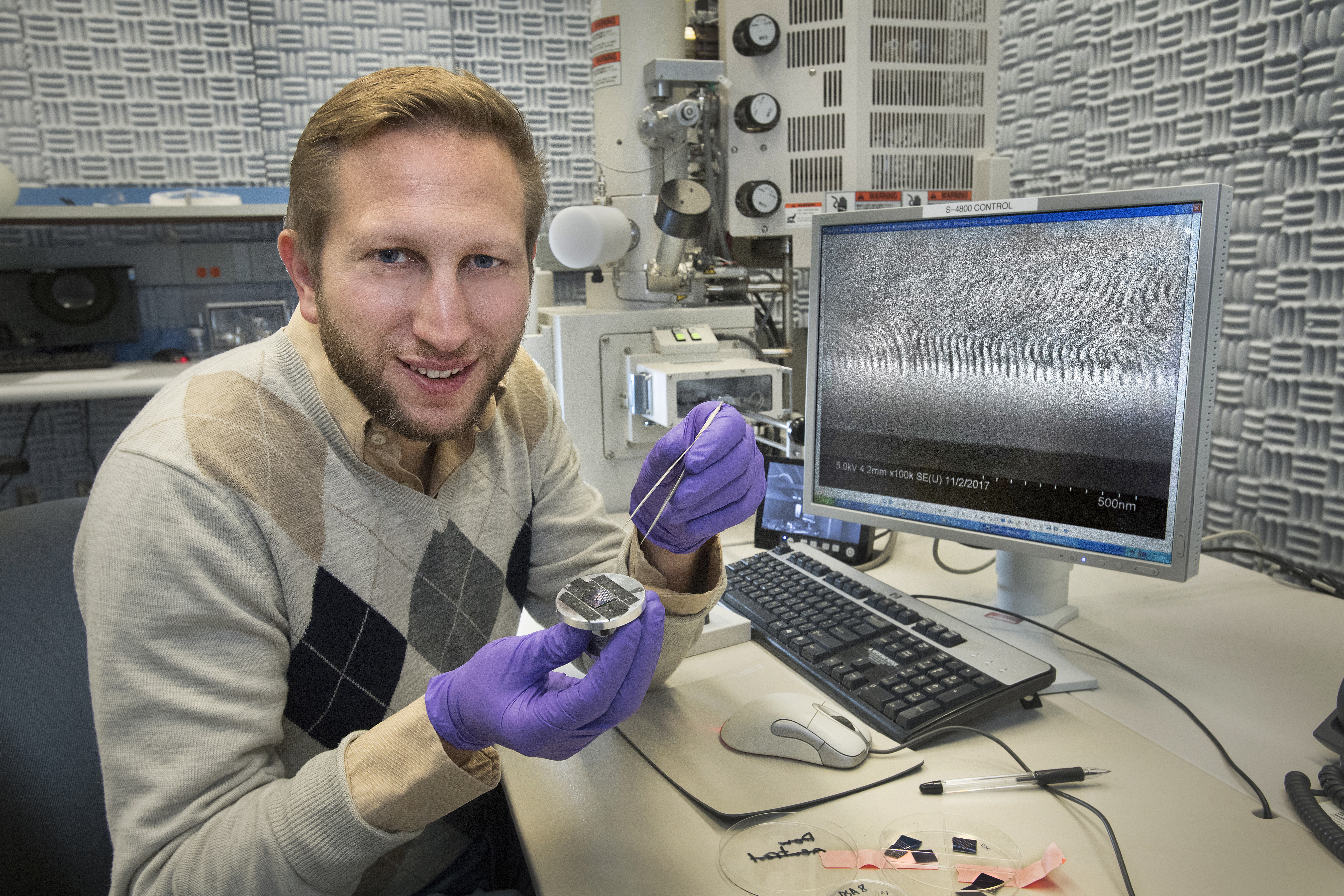
Materials scientist Gregory Doerk preparing a sample for electron microscopy at Brookhaven Lab's Center for Functional Nanomaterials. The scanning electron microscope image on the computer screen shows a cross-sectional view of line patterns transferred into a layer of silicon dioxide.
The ability to quickly generate ultra-small, well-ordered nanopatterns over large areas on material surfaces is critical to the fabrication of next-generation technologies in many industries, from electronics and computing to energy and medicine. For example, patterned media, in which data are stored in periodic arrays of magnetic pillars or bars, could significantly improve the storage density of hard disk drives.
Scientists can coax thin films of self-assembling materials called block copolymers—chains of chemically distinct macromolecules (polymer “blocks”) linked together—into desired nanoscale patterns through heating (annealing) them on a substrate. However, defective structures that deviate from the regular pattern emerge early on during self-assembly.
The presence of these defects inhibits the use of block copolymers in the nanopatterning of technologies that require a nearly perfect ordering—such as magnetic media, computer chips, antireflective surfaces, and medical diagnostic devices. With continued annealing, the block copolymer patterns can reconfigure to remove the imperfections, but this process is exceedingly slow. The polymer blocks do not readily mix with each other, so they must overcome an extremely large energy barrier to reconfigure.
Adding small things with a big impact
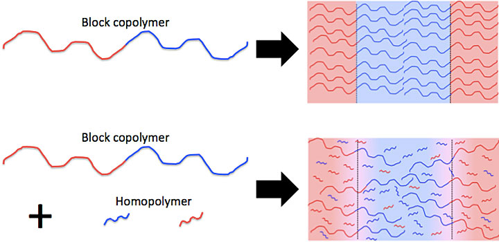
As shown in the illustration, a block copolymer consists of different molecule chains (red and blue) linked together; a homopolymer chain consists of identical molecules (red or blue). In this study, scientists blended a block copolymer containing two chemically distinct "blocks" with significantly smaller homopolymers from each of these blocks.
Now, scientists from the Center for Functional Nanomaterials (CFN)—a U.S. Department of Energy (DOE) Office of Science User Facility at Brookhaven National Laboratory—have come up with a way to massively speed up the ordering process. They blended a line-forming block copolymer with significantly smaller polymer chains made of only one type of molecule (homopolymers) from each of the two constituent blocks. The electron microscopy images they took after annealing the films for only a few minutes show that the addition of these two smaller homopolymers dramatically increases the size of well-ordered line-pattern areas, or “grains.”
“Without the homopolymers, the same block copolymer cannot produce grains with these sizes,” said CFN materials scientist Gregory Doerk, who led the work, which was published online in an ACS Nano paper on December 1. “Blending in homopolymers that are less than one-tenth of the size of the block copolymer greatly accelerates the ordering process. In the resulting line patterns, there is a constant spacing between each of the lines, and the same directions of line-pattern orientations—for example, vertical or horizontal—persist over longer distances.”
Doerk and coauthor Kevin Yager, leader of the Electronic Nanomaterials Group at CFN, used image analysis software to calculate the grain size and repeat spacing of the line patterns.
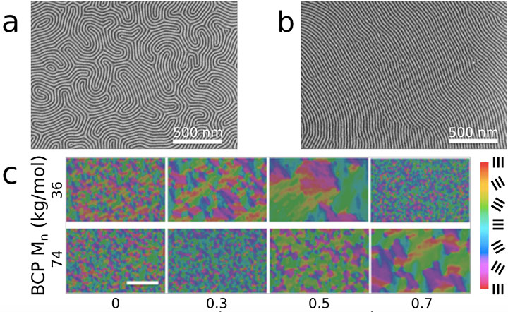
The scanning electron microscope images taken after thermal annealing at around 480 degrees Fahrenheit for five minutes show that the block copolymer/homopolymer blend generates a line pattern with a significantly higher degree of long-range order (b) than the unblended version (a), which shows a fingerprint-like pattern. Using image analysis software, the scientists generated colored maps to visualize the local line-pattern orientations in two block copolymers of different size (c). For both block copolymers, the size of well-ordered areas (indicated by the large individual colored regions, with the different line orientations designated by the corresponding color key) increases as more homopolymer is blended, up until a certain point, after which the pattern becomes disordered.
While blending different concentrations of homopolymer to determine how much was needed to achieve the accelerated ordering, they discovered that the ordering sped up as more homopolymer was added. But too much homopolymer actually resulted in disordered patterns.
“The homopolymers accelerate the self-assembly process because they are small enough to uniformly distribute throughout their respective polymer blocks,” said Doerk. “Their presence weakens the interface between the two blocks, lowering the energy barrier associated with the block copolymer reconfiguring to remove the defects. But if the interface is weakened too much through the addition of too much homopolymer, then the blocks will mix together, resulting in a completely disordered phase.”
Guiding the self-assembly of useful nanopatterns in minutes
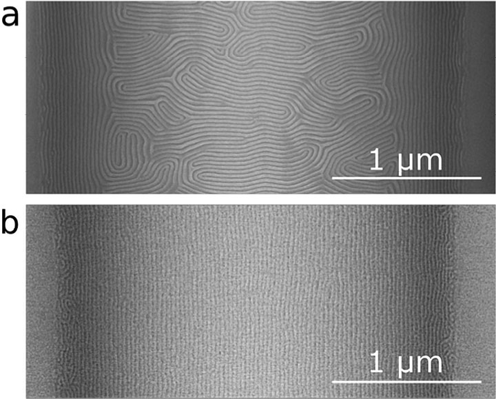
The unblended block copolymer aligns well close to the template guides ("sidewalls"), but this alignment degrades further in, as evident by the appearance of the fingerprint-like pattern in the center of the scanning electron microscope image in (a). Under the same annealing temperature and time (two minutes), the block copolymer/homopolymer blend retains the alignment across the entire area between the sidewalls (b).
To demonstrate how the rapid ordering in the blended system could accelerate the self-assembly of well-aligned nanopatterns over large areas, Doerk and Yager used line-pattern templates they had previously prepared through photolithography. Used to build almost all of today’s digital devices, photolithography involves projecting light through a mask (a plate containing the desired pattern) that is positioned over a wafer (usually made of silicon) coated with a light-sensitive material. This template can then be used to direct the self-assembly of block copolymers, which fill in the spaces between the template guides. In this case, after only two minutes of annealing, the polymer blend self-assembles into lines that are aligned across these gaps. However, after the same annealing time, the unblended block copolymer self-assembles into a mostly unaligned pattern with many defects between the gaps.
“The width of the gaps is more than 80 times the repeat spacing, so the fact that we got this degree of alignment with our polymer blend is really exciting because it means we can use templates with huge gaps, created with very low-resolution lithography,” said Doerk. “Typically, expensive high-resolution lithography equipment is needed to align block copolymer patterns over this large of an area.”
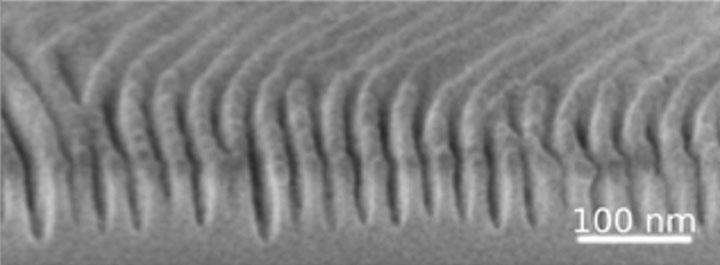
A scanning electron microscope image showing a cross-sectional view of the line patterns transferred into a silicon dioxide layer.
For these patterns to be useful for many nanopatterning applications, they often need to be transferred to other more robust materials that can withstand harsh manufacturing processes—for example, etching, which removes layers from silicon wafer surfaces to create integrated circuits or make the surfaces antireflective. In this study, the scientists converted the nanopatterns into a metal-oxide replica. Through chemical etching, they then transferred the replica pattern into a silicon dioxide layer on a silicon wafer, achieving clearly defined line patterns.
Doerk suspects that blending homopolymers with other block copolymers will similarly yield accelerated assembly, and he is interested in studying blended polymers that self-assemble into more complicated patterns. The x-ray scattering capabilities at the National Synchrotron Light Source II—another DOE Office of Science User Facility at Brookhaven—could provide the structural information needed to conduct such studies.
“We have introduced a very simple and easily controlled way of immensely accelerating self-assembly,” concluded Doerk. “Our approach should substantially reduce the number of defects, helping to meet the demands of the semiconductor industry. At CFN, it opens up possibilities for us to use block copolymer self-assembly to make some of the new functional materials that we envision.”
Brookhaven National Laboratory is supported by the Office of Science of the U.S. Department of Energy. The Office of Science is the single largest supporter of basic research in the physical sciences in the United States, and is working to address some of the most pressing challenges of our time. For more information, please visit science.energy.gov.
Follow @BrookhavenLab on Twitter or find us on Facebook.
2017-12648 | INT/EXT | Newsroom