- Home
- Facilities
- Research
-
Working at CFN
- Arrival & Departure
- Reports & Publications
- Acknowledging Use of CFN Facilities
- Data Management
- The Guide to Brookhaven
Safety Procedures
- Operations Plan
- Experimental Safety Reviews (ESR)
- COSA Training
- Hours of Operation
- Laser System Qualification
- Transport of Hazardous Materials
- Vendor On-site Scheduling Procedure (PDF)
- Electrical Equipment Inspections
- News & Events
- People
- Jobs
- Contact
- Business
- Intranet
Electronic Nanomaterials
Precision design and fabrication of nanoarchitectures
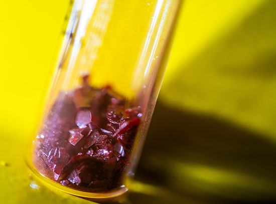
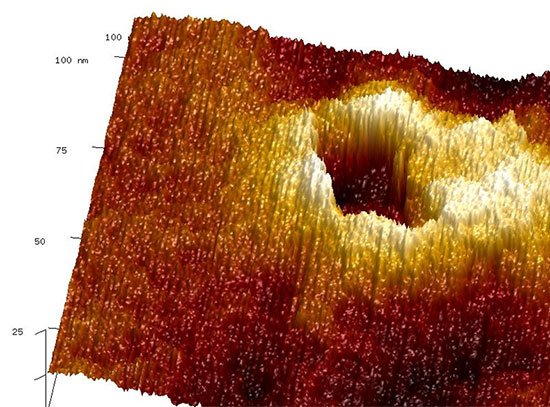
Functional properties arise from a material’s organization at the molecular and nanoscale. By precisely controlling nanoarchitectures, we can realize new electronic, optical, and quantum properties. Through our research program in electronic nanomaterials, we design and fabricate nanoarchitectures using nanofabrication, polymer-based self-assembly, layered stacking of two-dimensional materials, and infiltration-based hybrid material synthesis. We deploy frontier x-ray probes to characterize these systems and leverage machine learning to accelerate discovery. Our advances pave the way toward next-generation materials for transistors, solar cells, light-emitting diodes, sensors, membranes, and other technologies.

Associated Group Facilities
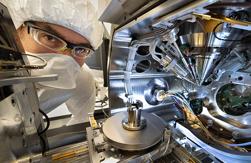
Nanofabrication Facility
The Nanofabrication Facility is housed in a class 100/1000 clean room dedicated to patterning and processing of thin films, nanomaterials, and devices. Instrumentation is capable of patterning a variety of materials over size scales ranging from 10 nanometers to 10 millimeters. The clean room is used to fabricate devices for nanoelectronics, nanophotonics, biomedical engineering, photovoltaics, x-ray optics, and nanomagnetics.
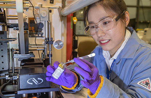
Synthesis and Characterization Facility
The Materials Synthesis and Characterization Facility includes laboratories for producing nanostructured materials and characterizing their basic structural, chemical and optical properties. The facility also supports infrastructure and expertise in solution-based processing of organic thin films, including tools for spin-casting, thermal processing, and UV/ozone treatment.
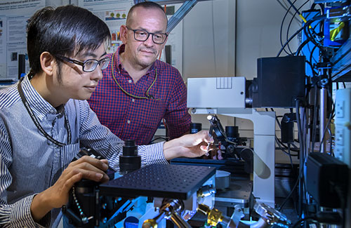
Advanced Optics Spectroscopy & Microscopy
A broad range of optical methods is available for characterization of energy transfer phenomena down to single molecular/particle level. Our capabilities include time- and spectrally resolved bulk/single molecule confocal fluorescence microscopy and fluorescence correlation spectroscopy.