Creating 'Movies' of Thin Film Growth at NSLS-II
Coherent x-rays at NSLS-II enable researchers to produce more accurate observations of thin film growth in real time
July 2, 2019
 enlarge
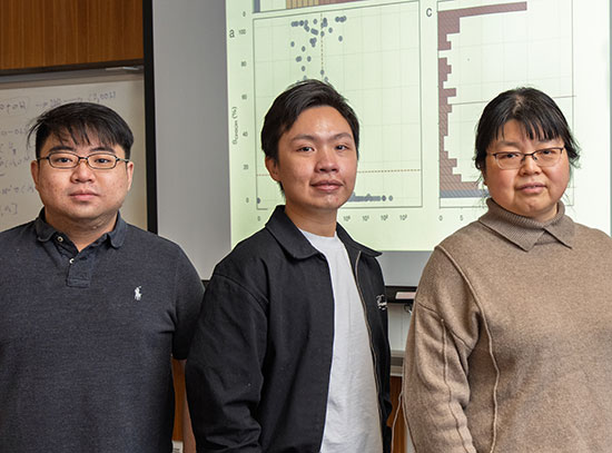
Co-authors Peco Myint (BU) and Jeffrey Ulbrandt (UVM) are shown at NSLS-II's CHX beamline, where the research was conducted.
From paint on a wall to tinted car windows, thin films make up a wide variety of materials found in ordinary life. But thin films are also used to build some of today’s most important technologies, such as computer chips and solar cells. Seeking to improve the performance of these technologies, scientists are studying the mechanisms that drive molecules to uniformly stack together in layers—a process called crystalline thin film growth. Now, a new research technique could help scientists understand this growth process better than ever before.
Researchers from the University of Vermont, Boston University, and the U.S. Department of Energy’s (DOE) Brookhaven National Laboratory have demonstrated a new experimental capability for watching thin film growth in real-time. Using the National Synchrotron Light Source II (NSLS-II)—a DOE Office of Science User Facility at Brookhaven—the researchers were able to produce a “movie” of thin film growth that depicts the process more accurately than traditional techniques can. Their research was published on June 14, 2019 in Nature Communications.
How thin films grow
This animation is a simplified representation of thin film growth. As C60 molecules are deposited onto a material, they form multiple layers simultaneously—not one layer at a time. After a molecule reaches the surface of the material, it migrates by surface diffusion towards the boundary of an existing layer, or the "step-edge," causing the step-edge to move out from the center of the mound. This process repeats as new layers are continuously formed in an organized pattern. The mound increases in height by one layer after an equivalent of one full layer of molecules has been deposited onto the material. The pattern of step-edges is self-similar after each full-layer-equivalent is deposited, just displaced one layer higher. The main result of the study is that this repeating self-similarity, or "autocorrelation," can be quantitatively measured with coherent x-rays, and that the autocorrelations can be used to deduce certain details of how step-edges propagate during the deposition.
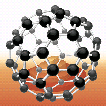
Like building a brick wall, thin films “grow” by stacking in overlapping layers. In this study, the scientists focused on the growth process of a nanomaterial called C60, which is popular for its use in organic solar cells.
“C60 is a spherical molecule that has the structure of a soccer ball,” said University of Vermont physicist Randall Headrick, lead author of the research. “There is a carbon atom at all of the corners where the ‘black’ and ‘white’ patches meet, for a total of 60 carbon atoms.”
Though spherical C60 molecules don’t perfectly fit side-by-side like bricks in wall, they still create a uniform pattern.
“Imagine you have a big bin and you fill it with one layer of marbles,” Headrick said. “The marbles would pack together in a nice hexagonal pattern along the bottom of the bin. Then, when you laid down the next layer of marbles, they would fit into the hollow areas between the marbles in the bottom layer, forming another perfect layer. We’re studying the mechanism that causes the marbles, or molecules, to find these ordered sites.”
But in real life, thin films don’t stack this evenly. When filling a bin with marbles, for example, you may have three layers of marbles on one side of the bin and only one layer on the other side. Traditionally, this nonuniformity in thin films has been difficult to measure.
“In other experiments, we could only study a single crystal that was specially polished so the whole surface behaved the same way at the same time,” Headrick said. “But that is not how materials behave in real life.”
Studying thin film growth through coherent x-rays
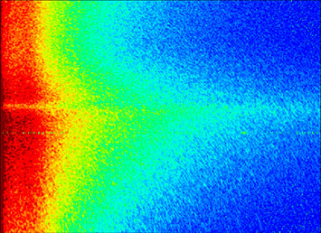
A snapshot of the speckle pattern "movie" produced at CHX. The speckles are most visible at the boundaries of each color.
To collect data that more accurately described thin film growth, Headrick went to the Coherent Hard X-ray Scattering (CHX) beamline at NSLS-II to design a new kind of experiment, one that made use of the beamline’s coherent x-rays. The team used a technique called x-ray photon correlation spectroscopy.
“Typically, when you do an x-ray experiment, you see average information, like the average size of molecules or the average distance between them. And as the surface of a material become less uniform or ‘rougher,’ the features you look for disappear,” said Andrei Fluerasu, lead beamline scientist at CHX and a co-author of the research. “What is special about CHX is that we can use a coherent x-ray beam that produces an interference pattern, which can be thought of like a fingerprint. As a material grows and changes, its fingerprint does as well.”
The “fingerprint” produced by CHX appears as a speckle pattern and it represents the exact arrangement of molecules in the top layer of the material. As layers continue to stack, scientists can watch the fingerprint change as if it were a movie of the thin film growth.
“That is impossible to measure with other techniques,” Fluerasu said.
Through computer processing, the scientists are able to convert the speckle patterns into correlation functions that are easier to interpret.
“There are instruments like high resolution microscopes that can actually make a real image of these kinds of materials, but these images usually only show narrow views of the material,” Headrick said. “A speckle pattern that changes over time is not as intuitive, but it provides us with data that is much more relevant to the real-life case.”
Co-author Lutz Wiegart, a beamline scientist at CHX, added, “This technique allows us to understand the dynamics of growth processes and, therefore, figure out how they relate to the quality of the films and how we can tune the processes.”
The detailed observations of C60 from this study could be used to improve the performance of organic solar cells. Moving forward, the researchers plan to use this technique to study other types of thin films as well.
 enlarge
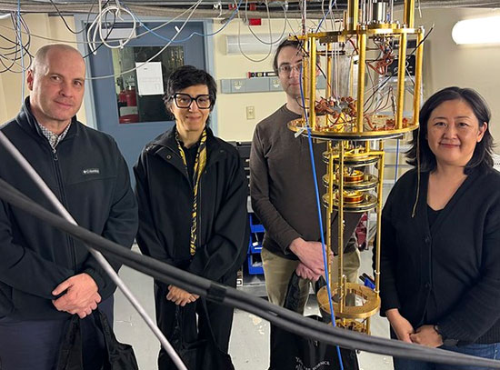
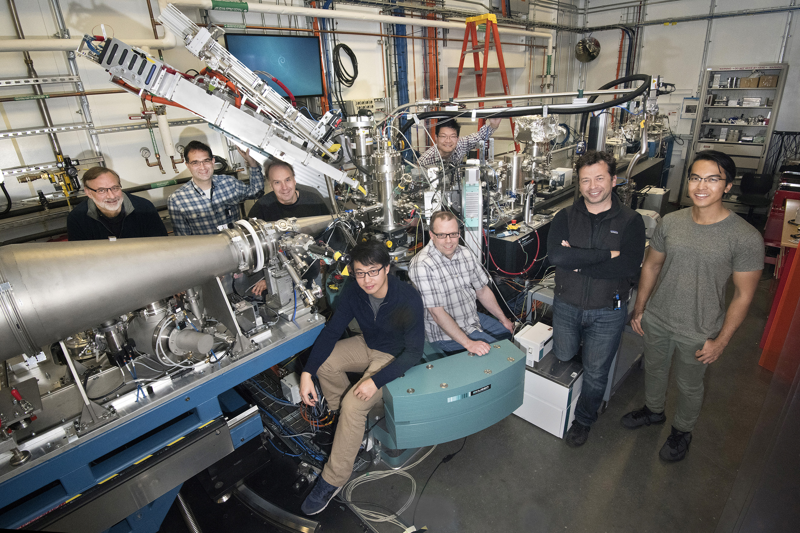
Members of the collaborating institutions are shown at NSLS-II's CHX beamline. Pictured from left to right are Karl F. Ludwig Jr. (BU), Lutz Wiegart (NSLS-II), Randall Headrick (UVM), Xiaozhi Zhang (UVM), Jeffrey Ulbrandt (UVM), Yugang Zhang (NSLS-II), Andrei Fluerasu (NSLS-II), and Peco Myint (BU).
This study was supported by DOE’s Office of Science and the National Science Foundation.
Brookhaven National Laboratory is supported by the U.S. Department of Energy’s Office of Science. The Office of Science is the single largest supporter of basic research in the physical sciences in the United States and is working to address some of the most pressing challenges of our time. For more information, visit https://energy.gov/science.
Follow @BrookhavenLab on Twitter or find us on Facebook.
2019-15581 | INT/EXT | Newsroom