Engineers Advance Insights on Black Phosphorus as a Material for Future Ultra-low Power Flexible Electronics
July 7, 2020
 enlarge
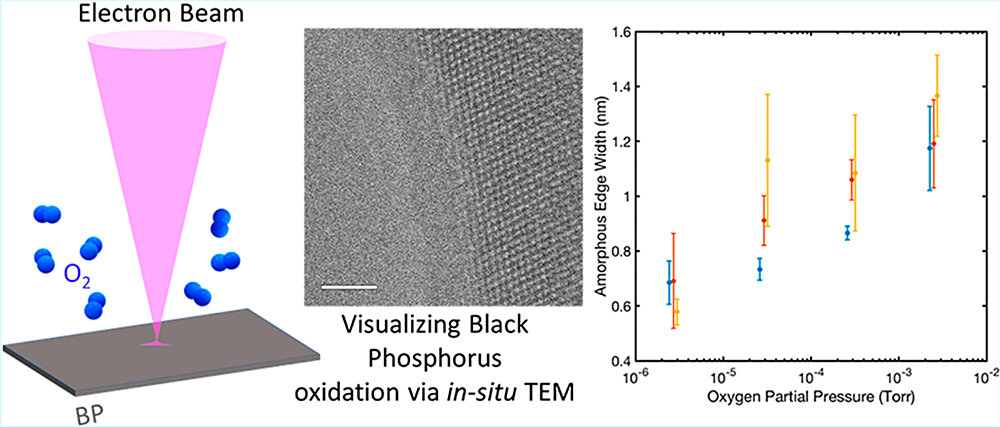
Using an environmental transmission electron microscope (ETEM) at Brookhaven Lab';s Center for Functional Nanomaterials, scientists visualized what happened as black phosphorous (BP) was exposed to oxygen gas (O2). A schematic of the experimental setup is shown on the left. The high-resolution TEM image (middle) captures the formation of an amorphous (i.e., lacking the long-range order characteristic of a crystalline material) phosphorous oxide (PxOy) layer (left side) at the exposed edge of the 2-D BP crystal (right side) during oxidation. The graph (right) shows the dependence of the thickness of the amorphous phosphorous oxide layer on oxygen pressure.
As described in this news release published by Vanderbilt University, scientists have captured for the first time the reaction of black phosphorous and oxygen at the atomic scale. Black phosphorous is a promising material for next-generation flexible electronics, but it degrades quickly when exposed to air. By performing environmental transmission electron microscopy (ETEM) in the Electron Microscopy Facility at the Center for Functional Nanomaterials (CFN)—a U.S. Department of Energy Office of Science User Facility at Brookhaven National Laboratory—the team observed in real time what happens when black phosphorous is exposed to oxygen. CFN staff scientist Dmitri Zakharov and CFN users from Vanderbilt performed the ETEM studies, reported in a paper published in Applied Materials & Interfaces. A fundamental understanding of the oxidation mechanism will ultimately help scientists develop strategies to mitigate degradation.
Black phosphorus is a crystalline material that is attracting growing research interest from semiconductor device engineers, chemists and material scientists to create high-quality atomically thin films.
From the perspective of a 2D layered material, black phosphorus shows promise for applications in next-generation flexible electronics that could enable advances in semiconductors, medical imaging, night vision and optical communication networks.
As a prospective graphene and silicon substitute, it has outstanding properties like tunable bandgap, which graphene lacks. A bandgap, an energy band in which no electron states can exist, is essential for creating the on/off flow of electrons that are needed in digital logic and for the generation of photons for LEDs and lasers.
Unfortunately, black phosphorus is hard to make and hard to keep. It degrades quickly when exposed to air. Why this happens and the exact mechanisms by which it happens—whether oxygen or moisture in the air degrade or both—remain a topic of active debate in the research community.

Piran Kidambi
Vanderbilt engineering researchers have shown for the first time that the reaction of black phosphorus to oxygen can be observed at the atomic scale using in situ-transmission electron microscopy (TEM). See YouTube videos.
The results are reported in their paper—Visualizing Oxidation Mechanisms in Few-Layered Black Phosphorus via In Situ Transmission Electron Microscopy—in the American Chemical Society’s Applied Materials & Interfaces journal.
“In research, a lot of times different and often contradictory hypothesis exist in the scientific community. However, the ability to observe a reaction at atomic resolution in real-time offers much needed clarity to propel advances. We are using the insights from our in-situ TEM experiments at atomic resolution in our lab to develop novel synthesis and preservation methods for black phosphorus,” said Piran Kidambi, assistant professor of chemical and biomolecular engineering.
“Current approaches have looked at encapsulating it with an oxide or polymer layer without really understanding why or how the oxidation proceeds,” said Andrew E. Naclerio, second year graduate student in the Department of Chemical and Biomolecular Engineering and the paper’s first author.

Andrew Naclerio
“Most understanding of black phosphorus oxidation has been based on results from spectroscopic probes,” said Kidambi, Naclerio’s adviser. In collaboration with Dmitri Zakharov, staff scientist at Brookhaven National Laboratory in Upton, New York, the team used environmental transmission electron microscopy (ETEM), which provides real time in-situ observation of structural information on a sample and reaction at atomic resolution.
“This is one of the few microscopes in the United States and the world with the capability to perform atomic resolution imaging while introducing gases and heating,” Kidambi said. The collaboration grew from a peer-reviewed user proposal and is funded by Department of Energy (DOE).
“Some insights we obtained were that the reaction proceeds via the formation of an amorphous layer that subsequently evaporates. Different crystallographic edges lead to varying degrees of etching and this agrees well will with theoretical calculations,” Kidambi said.
The collaboration for theoretical calculations with two of the paper’s authors, researchers Jeevesh Kumar and Mayank Shrivastava at the Indian Institute of Science in Bangalore, was formed at a conference where Kidambi was invited to give a talk.
The team aim to synthesize atomically thin films of black phosphorus using chemical vapor deposition, and insights on oxidation can be used to develop effective passivation techniques.
The Kidambi Research Group in the School of Engineering’s Department of Chemical and Biomolecular Engineering is affiliated with the Vanderbilt Institute of Nanoscale Science and Engineering (VINSE), the Interdisciplinary Materials Science Program and the Vanderbilt University Data Science Institute.
This research was funded by the U.S. Department of Energy and a Petroleum Research Fund grant from the American Chemical Society.
Contact: Brenda Ellis, 615 343-6314
brenda.ellis@vanderbilt.edu
2020-17315 | INT/EXT | Newsroom


