- Home
- Facilities
- Research
-
Working at CFN
- Arrival & Departure
- Reports & Publications
- Acknowledging Use of CFN Facilities
- Data Management
- The Guide to Brookhaven
Safety Procedures
- Operations Plan
- Experimental Safety Reviews (ESR)
- COSA Training
- Hours of Operation
- Laser System Qualification
- Transport of Hazardous Materials
- Vendor On-site Scheduling Procedure (PDF)
- Electrical Equipment Inspections
- News & Events
- People
- Jobs
- Contact
- Business
- Intranet
Electron Microscopy Facility
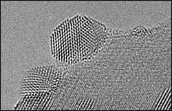
This facility consists of five top-of-the line transmission electron microscopes, two of which are highly specialized instruments capable of extreme levels of resolution, achieved through spherical aberration correction. The facility is also equipped with extensive sample-preparation capabilities. The scientific interests of the staff focus on understanding the microscopic origin of the physical and chemical behavior of materials, with specific emphasis on in-situ studies of materials in native, functional environments.
- Atomic-resolution imaging of internal materials structure with scanning transmission and transmission electron microscopy
- Spectroscopic characterization with energy dispersive x-ray spectroscopy and electron energy loss spectroscopy. Real time studies of processing / structure / property relationships in nanostructured materials, including in liquid and gaseous environments
Instrument Details
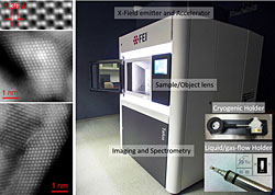
FEI Titan 80-300, a dedicated Environmental Transmission Electron Microscope (E-TEM)
Contact: Dmitri Zakharov
 This instrument is the first 80-300kV
field-emission environmental transmission electron
microscope to be installed in the US with an
objective-lens aberration corrector. It has a
spatial resolution of 0.08nm in the high-resolution
phase contrast mode, and can achieve
this resolution at unusually high pressures due to
the differential pumping apertures and custom
pumping arrangement that is incorporated with the
system. The maximum gas pressure for the
environmental-cell is about 20mbar for N2,
with other maximum pressures dependent on the atomic
weight of the gas. As a result, this instrument is
uniquely well-suited to image the fundamental
mechanisms of catalysis and catalyzed nanostructure
growth. The instrument also has scanning
transmission imaging (STEM), magnetic imaging, and
chemical analysis capabilities. In addition, a Lorentz
lens and a bi-prism allows imaging electrostatic and
magnetic potentials or fields in materials. The FEI
Titan is
also equipped with an energy dispersive x-ray
spectrometer and an electron energy-loss image
filter spectrometer. A mass-flow controlled
catalytic reaction system capable of providing
controlled pressures of gas mixtures will be
installed in the near future.
This instrument is the first 80-300kV
field-emission environmental transmission electron
microscope to be installed in the US with an
objective-lens aberration corrector. It has a
spatial resolution of 0.08nm in the high-resolution
phase contrast mode, and can achieve
this resolution at unusually high pressures due to
the differential pumping apertures and custom
pumping arrangement that is incorporated with the
system. The maximum gas pressure for the
environmental-cell is about 20mbar for N2,
with other maximum pressures dependent on the atomic
weight of the gas. As a result, this instrument is
uniquely well-suited to image the fundamental
mechanisms of catalysis and catalyzed nanostructure
growth. The instrument also has scanning
transmission imaging (STEM), magnetic imaging, and
chemical analysis capabilities. In addition, a Lorentz
lens and a bi-prism allows imaging electrostatic and
magnetic potentials or fields in materials. The FEI
Titan is
also equipped with an energy dispersive x-ray
spectrometer and an electron energy-loss image
filter spectrometer. A mass-flow controlled
catalytic reaction system capable of providing
controlled pressures of gas mixtures will be
installed in the near future.
FEI Talos 200x an operando Scanning Transmission Electron Microscope
Contact: Kim Kisslinger
 The FEI Talos F200X is a high-resolution
analytical scanning/transmission electron microscope
(S/TEM) that is routinely operated at 200 keV. This
microscope is equipped with an X-FEG electron source
module that gives a source brightness four times
that of a Schottky FEG emitter. This high source
brightness enables near diffraction limited imaging
and dramatically improves the spectroscopic
performance. In addition to the extra-bright gun, it
combines outstanding high-resolution
scanning/transmission electron microscope and TEM
imaging with a four-quadrant 0.9-sr energy
dispersive X-ray spectrometer (EDS) for elemental
and compositional mapping. Talos F200X allows for
the fastest and most precise EDS analysis in all
dimensions, along with HRTEM imaging with fast
navigation for in-situ microscopy. The
instrument is custom designed to have an
objective-area pressure interlock and differential
pumping capabilities close to the gun to protect the
field emitter from any gas leakage event. Due to
this protection feature, gas- and liquid-cell operando holders
can be readily used in this system to study reaction
dynamics under liquid and gas environments.
The FEI Talos F200X is a high-resolution
analytical scanning/transmission electron microscope
(S/TEM) that is routinely operated at 200 keV. This
microscope is equipped with an X-FEG electron source
module that gives a source brightness four times
that of a Schottky FEG emitter. This high source
brightness enables near diffraction limited imaging
and dramatically improves the spectroscopic
performance. In addition to the extra-bright gun, it
combines outstanding high-resolution
scanning/transmission electron microscope and TEM
imaging with a four-quadrant 0.9-sr energy
dispersive X-ray spectrometer (EDS) for elemental
and compositional mapping. Talos F200X allows for
the fastest and most precise EDS analysis in all
dimensions, along with HRTEM imaging with fast
navigation for in-situ microscopy. The
instrument is custom designed to have an
objective-area pressure interlock and differential
pumping capabilities close to the gun to protect the
field emitter from any gas leakage event. Due to
this protection feature, gas- and liquid-cell operando holders
can be readily used in this system to study reaction
dynamics under liquid and gas environments.
JEOL JEM-1400 LaB6 120 KV Transmission Electron Microscope
Contact: Fernando Camino
The JEOL JEM-1400 LaB6 120 kV transmission electron microscope is an easy-to-use, high contrast instrument with excellent imaging (TEM and STEM modes) and analytical (energy dispersive spectroscopy detector) capabilities. With an easily changeable accelerating voltage range of 40-120 keV, the JEM-1400 TEM is highly suitable for polymer, biological, and materials science applications. Usually, after one training session, users unfamiliar with electron microscopy can use the instrument independently for TEM imaging purposes.
TEM Sample Preparation Facilities
Contact: Kim Kisslinger
Sample preparation is a critical and often underestimated aspect of transmission electron microscopy. Sample preparation for TEM can be a complex and involved procedure drawing upon a variety of mechanical and non-mechanical methods. The method chosen for TEM sample preparation is highly specific to the material to be analyzed and the desired information to be attained. Thin high quality TEM samples should have a thickness that is roughly equal to the mean free path electrons that transmit through the sample, which may only be a few tens of nanometers. The CFN maintains an array of equipment enabling a variety of standard TEM sample preparation capabilities. While users are generally expected to carry out their own specimen preparation, guidance and expertise may be provided by CFN electron microcopy staff.
Image Analysis Facility
The EM Group has a full range of image processing and analysis software for the interpretation of data. These includes, one 4-core, dual quad MacPro, equipped with MacTempas (for HREM/STEM image simulation and exit-wave reconstruction), CrystalKit and Adobe Photoshop (Fovea Pro Image analysis plug-ins) and one 4-core dual-quad PC with Digital Micrograph, True Image (exit wave reconstruction), and Inspect3D / Amira (tomographic reconstruction).
Analytical Bio/Soft Matter Transmission Electron Microscope (TEM)
JEOL 1400 TEM:
The JEOL JEM-1400 LaB6 120 kV transmission electron microscope is an easy-to-use, high contrast instrument with excellent imaging (TEM and STEM modes) and analytical (energy dispersive spectroscopy detector) capabilities.
Environmental Transmission Electron Microscope (E-TEM)
Titan 80-300:
The E-TEM instrument (FEI Titan 80-300) is an 80 – 300 kV field-emission transmission electron microscope with an objective-lens aberration corrector at spatial resolution of 0.08 nm. The instrument has scanning transmission imaging, magnetic imaging, and chemical analysis capabilities.
FEI TALOS Operando S/TEM
FEI TALOS:
The FEI Talos F200X is a high-resolution analytical scanning/transmission electron microscope (S/TEM) that is routinely operated at 200 keV. This microscope is equipped with an X-FEG electron source module that gives a source brightness four times that of a Schottky FEG emitter.
AJA UHV Dual E-beam Evaporator for Metals
The AJA ultra-high-vacuum (UHV) electron-beam (e-beam) evaporator is a dedicated thin-film deposition system for the growth of high-quality metallic and alloy thin films for TEM experiments and related nanoscience applications. The system is optimized for the deposition of single-crystalline and polycrystalline metal/alloy thin films under ultra-high-vacuum conditions and elevated substrate temperatures.