Scientists Detect Unusual ‘Quasiparticles’ in Tri-Layer Graphene
Findings reveal new possibilities for manipulating charge and spin in electronic devices
September 25, 2011
By studying three layers of graphene — sheets of honeycomb-arrayed carbon atoms — stacked in a particular way, scientists at the U.S. Department of Energy’s Brookhaven National Laboratory have discovered a “little universe” populated by a new kind of “quasiparticles” — particle-like excitations of electric charge. Unlike massless photon-like quasiparticles in single-layer graphene, these new quasiparticles have mass, which depends on their energy (or velocity), and would become infinitely massive at rest.
That accumulation of mass at low energies means this trilayer graphene system, if magnetized by incorporating it into a heterostructure with magnetic material, could potentially generate a much larger density of spin-polarized charge carriers than single-layer graphene — making it very attractive for a new class of devices based on controlling not just electric charge but also spin, commonly known as spintronics.
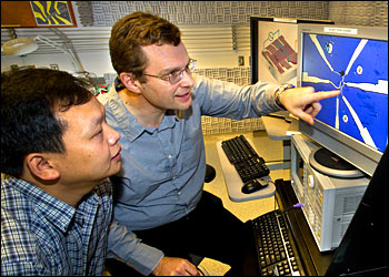
“Our research shows that these very unusual quasiparticles, predicted by theory, actually exist in three-layer graphene, and that they govern properties such as how the material behaves in a magnetic field — a property that could be used to control graphene-based electronic devices,” said Brookhaven physicist Igor Zaliznyak, who led the research team. Their work measuring properties of tri-layer graphene as a first step toward engineering such devices was published online in Nature Physics on September 25, 2011.
Graphene has been the subject of intense research since its discovery in 2004, in particular because of the unusual behavior of its electrons, which flow freely across flat, single-layer sheets of the substance. Stacking layers changes the way electrons flow: Stacking two layers, for example, provides a “tunable” break in the energy levels the electrons can occupy, thus giving scientists a way to turn the current on and off. That opens the possibility of incorporating the inexpensive substance into new types of electronics.
With three layers, the situation gets more complicated, scientists have found, but also potentially more powerful.
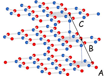
One important variable is the way the layers are stacked: In “ABA” systems, the carbon atoms making up the honeycomb rings are directly aligned in the top and bottom layers (A) while those in the middle layer (B) are offset; in “ABC” variants, the honeycombs in each stacked layer are offset, stepping upwards layer by layer like a staircase. So far, ABC stacking appears to give rise to more interesting behaviors — such as those that are the subject of the current study.
For this study, the scientists created the tri-layer graphene at the Center for Functional Nanomaterials (CFN) at Brookhaven Lab, peeling it from graphite, the form of carbon found in pencil lead. They used microRaman microscopy to map the samples and identify those with three layers stacked in the ABC arrangement. Then they used the CFN’s nanolithography tools, including ion-beam milling, to shape the samples in a particular way so they could be connected to electrodes for measurements.
At the National High Magnetic Field Laboratory (NHMFL) in Tallahassee, Florida, the scientists then studied the material’s electronic properties — specifically the effect of an external magnetic field on the transport of electronic charge as a function of charge carrier density, magnetic field strength, and temperature.
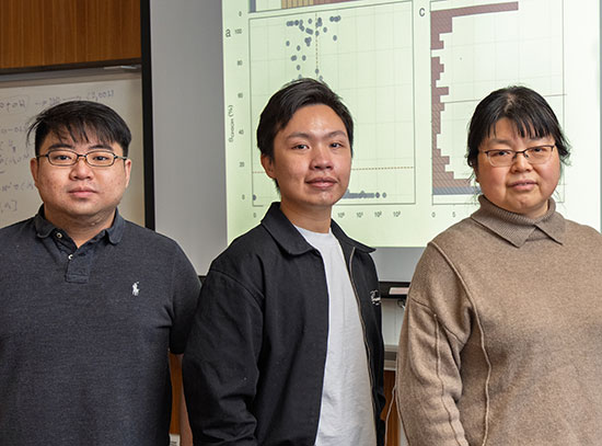
“Ultimately, the success of this project relied on hard work and rare experimental prowess of talented young researchers with whom we engaged in these studies, in particular, Liyuan Zhang, who at the time was research associate at Brookhaven, and Yan Zhang, then a graduate student from Stony Brook University,” said Igor Zaliznyak.
The measurements provide the first experimental evidence for the existence of a particular type of quasiparticle, or electronic excitation that acts like a particle and serves as a charge carrier in the tri-layer graphene system. These particular quasiparticles, which were predicted by theoretical studies, have ill-defined mass — that is, they behave as if they have a range of masses — and those masses diverge as the energy level decreases with quasiparticles becoming infinitely massive.
Ordinarily such particles would be unstable and couldn’t exist due to interactions with virtual particle-hole pairs — similar to virtual pairs of oppositely charged electrons and positrons, which annihilate when they interact. But a property of the quasiparticles called chirality, which is related to a special flavor of spin in graphene sytems, keeps the quasiparticles from being destroyed by these interactions. So these exotic infinitively massive particles can exist.
“These results provide experimental validation for the large body of recent theoretical work on graphene, and uncover new exciting possibilities for future studies aimed at using the exotic properties of these quasiparticles,” Zaliznyak said.
For example, combining magnetic materials with tri-layer graphene could align the spins of the charge-carrier quasiparticles. “We believe that such graphene-magnet heterostructures with spin-polarized charge carriers could lead to real breakthroughs in the field of spintronics,” Zaliznyak said.
This research was funded primarily by the DOE Office of Science (BES); work at the NHMFL was funded by the National Science Foundation and the State of Florida.
The Center for Functional Nanomaterials at Brookhaven National Laboratory is one of the five DOE Nanoscale Science Research Centers (NSRCs), premier national user facilities for interdisciplinary research at the nanoscale. Together the NSRCs comprise a suite of complementary facilities that provide researchers with state-of-the-art capabilities to fabricate, process, characterize and model nanoscale materials, and constitute the largest infrastructure investment of the National Nanotechnology Initiative. The NSRCs are located at DOE’s Argonne, Brookhaven, Lawrence Berkeley, Oak Ridge and Sandia and Los Alamos national laboratories. For more information about the DOE NSRCs, please visit http://nano.energy.gov.
2011-2597 | INT/EXT | Newsroom


