Research
Our research focuses on light–matter interactions in low-dimensional semiconductor nanomaterials, including hybrid systems and heterostructures, with particular emphasis on interfacial charge and energy transfer. A central objective is to understand how energy and charge carriers are transported across interfaces and to develop strategies for controlling these processes through self-assembly and electronic bandgap engineering.
- Valley Polarization in Heterostructures
We aim to develop two-dimensional transition metal dichalcogenide (TMD) heterostructures capable of sustaining optically induced valley polarization at room temperature. We have demonstrated that chiral perovskites can function as efficient spin filters, enabling selective valley population in TMDs via chiral-induced spin-selective charge transfer at room temperature (Nature Communications, 2023). More recently, our efforts have expanded to the use of chiral II–IV semiconductor nanocrystals to induce and stabilize valley polarization in monolayer TMDs under ambient conditions.
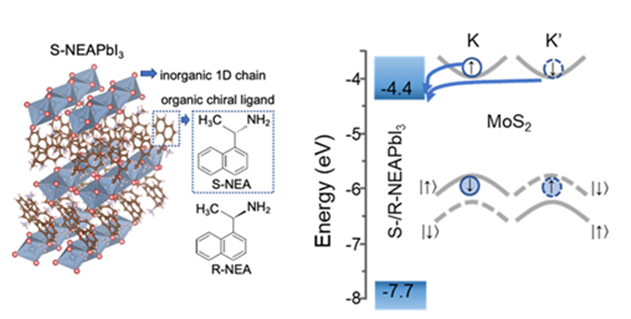
Figure caption: Heterostructure composed of a chiral one-dimensional perovskite and a monolayer TMD (left), and the corresponding band alignment favoring spin-selective charge transfer from the TMD to the chiral perovskite (right). Reproduced from Nature Communications 14, 5234 (2023).
Interfacial Charge Transfer in 2D TMD Heterostructures
Our group has contributed extensively to understanding interfacial charge and energy transfer in two-dimensional heterostructures. Two recent perspective articles in ACS Applied Optical Materials (2023) and ACS Energy Letters (2019) highlight optical studies from our group and others addressing these processes in the context of sensing, optoelectronics, and quantum information science.
We have developed colloidal quantum dot–TMD heterostructures for chemical sensing and solar energy harvesting (Advanced Functional Materials, 2018), as well as 2D heterostructures with tunable charge and energy transfer achieved through bandgap engineering (ACS Nano, 2016, 2019; ACS Omega, 2026). We have also demonstrated heterostructures exhibiting cascaded energy transfer that mimics natural light-harvesting systems (ACS Photonics, 2019). In addition, we have employed conductive polymers to fabricate TMD-based photodetectors with enhanced sensitivity enabled by nanoscale polymer patterning (ACS Photonics, 2018), and perovskite nanowires to create polarization-sensitive graphene photodetectors (Wiley PPSC, 2018).
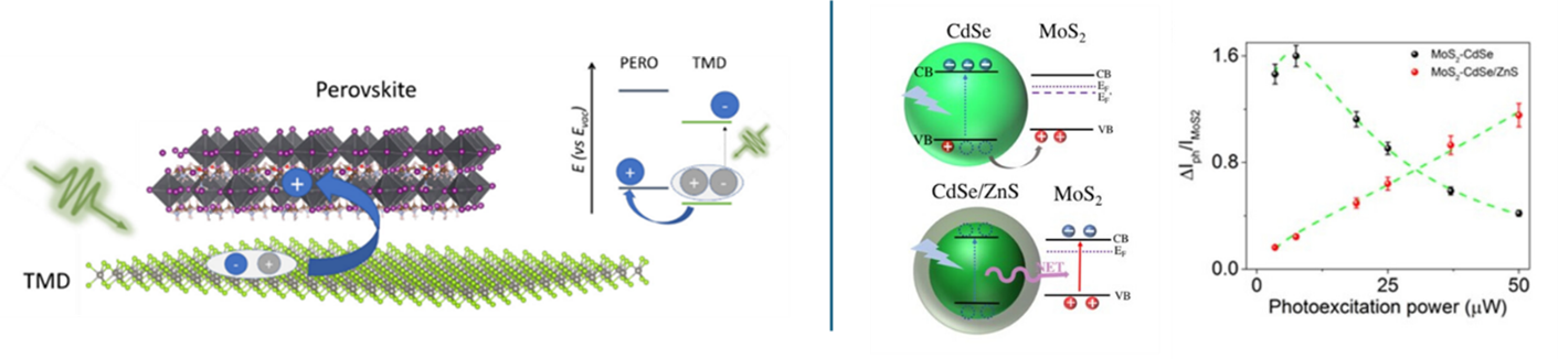
Figure caption: (Left) Perovskite–monolayer TMD heterostructure exhibiting interfacial charge transfer, with band alignment favoring hole transfer from the TMD to the perovskite. (Right) Bandgap engineering of quantum dot–TMD heterostructures enabling selective charge or energy transfer. Adapted from ACS Advanced Optical Materials (2023).
- Nanoscale Photoinduced Charge Transfer at the Single-Quantum-Dot Level
We have long been active in the study of photoinduced charge transfer at the single-nanoparticle and single-molecule level using colloidal quantum dots (QDs). A perspective article from our group (ACS Omega, 2019) summarizes work by us and others on the kinetics and dynamics of these processes in QDs and hybrid systems.
Using surface-based self-assembly, we fabricated donor–bridge–acceptor QD dimers with systematically varied bridge lengths, enabling controlled electron-transfer rates (Angewandte Chemie International Edition, 2011; Small, 2012). We also demonstrated QD–conjugated polymer hybrids with tunable hole-transfer rates by engineering core/shell QDs with different shell thicknesses. In a series of studies, we investigated emission intermittency (“blinking”) of isolated CdSe QDs under applied external electric fields, demonstrating reversible modulation of QD emission (ACS Nano, 2012; Chemical Communications, 2014; Nanoscale, 2015; in collaboration with Mathew Maye, Syracuse University).
More recently, we addressed challenges associated with near-infrared single-particle spectroscopy of lead halide QDs, including photoinduced charge transfer to TiO₂ and the generation of hot excitons (Nanoscale, 2017; Chemical Communications, 2018). Using single-particle detection, we also demonstrated energy transfer between isolated QDs and monolayer and few-layer indirect-bandgap TMDs such as SnS₂ (ACS Nano, 2016).
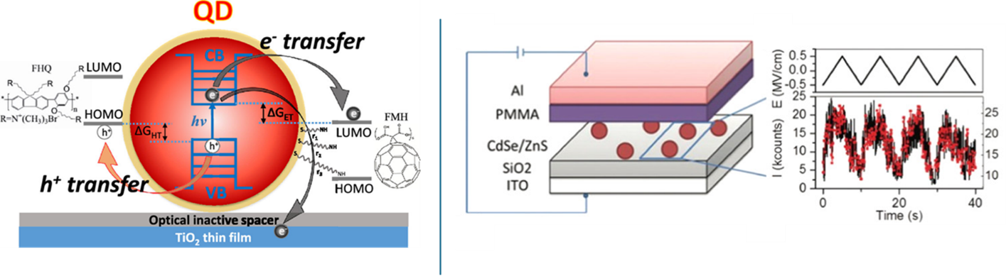
Figure caption: (Left) Photoinduced charge transfer in a QD hybridized with various acceptors. (Right) Isolated QDs embedded in a capacitor structure exhibit reversible emission changes under an applied external electric field. Adapted from ACS Omega (2019).
- Plasmonic Quantum Dots with Regulated Optical Output
In collaboration with Oleg Gang (CFN, BNL / Columbia University), we exploit DNA-based self-assembly to construct supramolecular architectures composed of quantum dots and noble-metal (gold) nanoparticles, with nanometer-scale control over interparticle spacing and geometry. These assemblies, ranging from simple dimers (Chemical Communications, 2010) to clusters (ACS Nano, 2015) and dumbbell-like structures (ACS Nano, 2020), exhibit rich optical phenomena, including controlled emission enhancement, collective plasmon–exciton coupling, and induced optical polarization.
- Advanced Optical Methods
Our group has developed a comprehensive suite of advanced ultrafast optical spectroscopies and microscopies with femtosecond temporal resolution and sub-diffraction-limited spatial resolution. These tools enable ex situ and in situ investigations of materials and biological systems at both room temperature and cryogenic temperatures. Capabilities include broadband femtosecond pump–probe transient absorption and reflectivity spectroscopy with cryogenic extension, femtosecond pump–probe absorption microscopy, time-resolved multidimensional confocal photoluminescence microscopy for quantum materials, cryogenic time-resolved spin-relaxation microscopy, and hyperspectral dark-field single-particle scattering microscopy.
More recently, we have implemented instrumentation for ultrafast optical characterization of defect emission and spin relaxation at cryogenic temperatures using magneto-optical techniques. Together, these capabilities enable detailed measurements of chirality- and spin-dependent properties in semiconductor materials. We invite interested researchers to visit the Advanced Optical Facility page to learn more about the unique instrumentation available through the CFN User Program and our publications page to learn about our group past research.