Resolution Limits of Electron-beam Lithography Pushed Towards the Atomic Scale
October 22, 2013
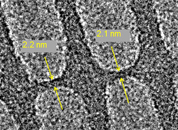
Electron microscopy image obtained of the written features (dark regions), fabricated using a scanning transmission electron microscope.
What Is The Scientific Achievement?
Electron-beam lithography (EBL) is a method of creating nanoscale patterns by exposing a resist to a focused source of electrons. We investigated the ultimate limits of EBL through the use of an aberration-corrected scanning transmission electron microscope (STEM). Optimization of electron exposure and resist development demonstrated the ability to create features of 2 nm in size – roughly 10 atoms wide. This is the highest resolution ever achieved with this technique.
Why Does This Matter?
EBL has been used for the last 50 years as method to pattern nanoscale features and devices, and it continues to be broadly used in nanotechnology and industrial applications. It is essential to the field of nanotechnology for its sub-10-nm resolution, arbitrary patterning capabilities and fast prototyping. The practical resolution limit of current EBL methods is near 10 nm, but the future of research in nanotechnology increasingly requires top-down control at the few nanometer length scale. It is expected that the development of EBL methods at this length will impact a wide array of fields, including excitonics, plasmonics, nanoscale optics, molecular electronics, the placement of biomolecules and templated self-assembly.
What Are The Specifics?
- Use of a high-brightness, aberration corrected scanning transmission electron microscope allowed patterning with a 0.15 nm electron beam.
- Extensive optimization of electron beam exposure and resist development yielded reproducible feature sizes of the order of 2 nm.
- The difference between the incident source size of 0.15 nm and the resulting pattern size of 2 nm demonstrates that the scattering of electrons in the resist leads to a fundamental limit on feature size achievable with electron beam lithography.
Reference
Resolution Limits of Electron-Beam Lithography toward the Atomic Scale
Vitor Manfrinato,1 Lihua Zhang,2 Dong Su,2 Huigao Duan,3 Richard Hobbs,1 Eric Stach2 and Karl Berggren,1
- Electrical Engineering and Computer Science Department, Massachusetts Institute of Technology
- Center for Functional Nanomaterials, Brookhaven National Laboratory
- Micro–Nano Technologies Research Center, Hunan University, China
Nano Letters ASAP, DOI: 10.1021/nl304715p (2013).
Acknowledgment of Support
This material is based upon work supported as part of the Center for Excitonics, an Energy Frontier Research Center funded by the U.S. Department of Energy, Office of Science, Office of Basic Energy Sciences under Award Number DE-SC0001088. The STEM lithography work was carried out at the Center for Functional Nanomaterials, Brookhaven National Laboratory, which is supported by the U.S. Department of Energy, Office of Basic Energy Sciences, under Contract No DE-AC02-98CH10886.
2013-4398 | INT/EXT | Newsroom