CFN User Spotlight: Dirk Englund Tracks Photons to Develop Unprecedented Quantum Technology
September 3, 2014
Dirk Englund
Quantum photonics research could change the way we communicate, compute, and measure phenomena on the smallest scales possible. To probe these processes and design new technology that operates with single-photon and single-electron precision, MIT physicist and professor Dirk Englund turns to the experts and instruments at Brookhaven Lab’s Center for Functional Nanomaterials. Englund, who leads the Quantum Photonics Group at MIT, explores the quantum landscape with an eye on applications ranging from cryptography to neurology.
What does your research on quantum photonics involve and why does it interest you?
My research focuses on controlling quantum states in photons and semiconductor spin systems to address problems in communication, computation, and metrology.
This field combines a few aspects that make it challenging, but also fun and gratifying. Quantum information combines principles from physics, mathematics, and computer science—three areas that I’ve always been interested in. By engineering things at the nanometer scale, we’re able to explore new ways to control quantum systems, in ways that just weren’t possible a decade or so ago. I think that the combination of fundamental discovery, together with the engineering aspect of developing useful—and potentially disruptive technologies—makes this field really exciting.
What first drew you to exploring quantum-scale phenomena and photonics?
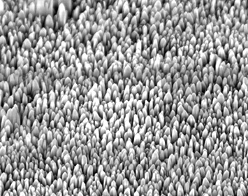
Nanoscale pillars etched from diamond to act as magnetic poles. Courtesy MIT.
I started college wanting to go into theoretical physics. But then I realized that I also really enjoyed building devices and doing experiments—particularly during my junior and senior years working in the quantum optics group of Hideo Mabuchi at Caltech. Quantum optics allows you explore strange phenomena in quantum mechanics, while also applying these phenomena to make useful devices and systems—that combination of discovery and material development was really appealing to me.
An example is quantum cryptography, where we can use the strange phenomenon of quantum entanglement to allow two people at a distance to communicate with proven security—this is not possible (or at least not known) under the laws of classical physics.
How does your research—and that of your students—impact the field of cryptography?
We’re building optical systems that use nonclassical light for cryptography. Secure communications is becoming increasingly important, but today’s public key crypto-systems rely on the presumed difficulty of solving certain mathematical problems—but they are not inherently secure. Quantum key distribution is the only provably secure way we know of to allow two parties to amplify some amount of secret information and then communicate securely. We hope to make quantum cryptography faster and more scalable by implementing devices into integrated optical chips—much like the chips that are now being developed by the likes of IBM and Intel for optical interconnects. In fact, we’ve actually been working very closely with scientists in IBM’s silicon photonics team—Dr. Solomon Assefa, in particular. The idea is to make quantum cryptography devices low-cost and scalable, and thereby make this form of secure communications practical.
What other technologies might be advanced by mastery of these quantum phenomena?
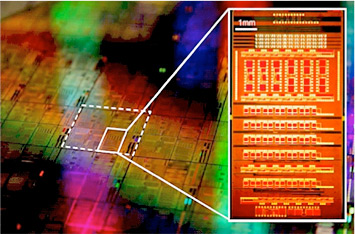
Silicon-based photonic circuits show promise for high-speed, high-efficiency computer chips.
Some of our work on integrated optics is aimed at simulating small quantum systems—such as the energy levels of small molecules—that are extremely difficult to solve using classical computers. This is because classical computers are very bad at representing quantum systems, as you can pretty easily see for yourself if you consider a small quantum system of n quantum bits (qubits). Because of the superposition principle and quantum entanglement, one would need more than about 2^n classical bytes just to represent this quantum system, let alone solve some property of it. In other words, the amount of classical information one needs to represent a quantum system scales exponentially with the size of that quantum system. For 60 or so qubits, we’d need on the order of one million terabytes of classical data to represent it. For 70 qubits, it’d be one billion terabytes. You can see that even for small numbers of qubits, classical computers very quickly become inadequate. On the other hand, a small quantum computer could solve these kinds of problems efficiently.
Also, small quantum systems can make excellent sensors. For example, working with collaborators in neuroscience, we’re trying to see if sensors consisting of two electrons trapped in nanometer-scale particles of diamond could be used to measure neuronal signals in the brain. These sensors use the spin state of these electrons, which respond very sensitively to external fields, a bit like watching the oscillations of tiny spinning tops.
What are the greatest challenges facing the development of such quantum photonic devices?
The ideas underpinning quantum information science are still very new, and indeed are active areas of research. Implementing these ideas requires new types of technologies, such as single photon sources, single photon detectors, and stable quantum memories that are still in the early stages of development. That shouldn’t be too surprising, considering we’ve been optimizing, say, combustion engines for hundreds of years, but we’ve only been working on exploiting quantum phenomena for a few decades at best. But it’s clear that these quantum technologies are very rapidly improving, and records are made every few months in many areas. I think that things will look very, very different 5-10 years from now. If history is any guide, things that seem really daunting now will seem pretty easy by then.
How do you see the landscape changing in that timeframe? What new things might we see?
- A small quantum system out-performing a classical computer at something, such as simulation
- Fairly practical, high-speed secure quantum communication systems
- A way to create entanglement between many quantum memories—this will produce new states of matter that will be very interesting to study and that could enable new kinds of applications
Beyond all that, history has shown that once you start engineering with new discoveries in physics, you actually develop a much better understanding of it, and that in turn drives new discoveries. So as we learn to engineer quantum systems like we’ve engineered motors and control systems, entirely new fields and applications will be discovered.
Given the considerable resources at MIT, why bring your research to the Center for Functional Nanomaterials?
When you work at the CFN, you’re surrounded by people who “speak” nanoscience. This concentration of expert knowledge in nanoscience promotes new discoveries and breakthroughs in a way that few other places can. Of course, the excellent (and well-maintained) equipment is also essential.
For my group, in particular, the CFN has been complementary to the university fabrication resources we have at MIT. At the CFN, we can do things that are very difficult or impossible in a normal university setting. Developing a radically new process, like our processing of diamond quantum memories, has been so successful at the CFN because of the consistency in the fabrication tools, the wide range of characterization tools, and the expert knowledge. After having developed a process, we can then translate it into other fabrication facilities. But it is in the process development itself where the CFN is just a really terrific resource for us.
What are some recent publications involving CFN collaboration that were particularly interesting or rewarding to you and your colleagues?
Here’s a short list:
- Scalable Fabrication of High Purity Diamond Nanocrystals with Long-Spin-Coherence Nitrogen Vacancy Centers, Nano Letters 14 (2013). In the News: NanoTechWeb, PhysicsWorld, Nature News Feature
- Chip-integrated ultrafast graphene photodetector with high responsivity, Nature Photonics 7, 883–887 (2013). In the news: MIT News, Nature, Gizmodo, Photonics.com, MIT Technology Review, NPR Marketplace
- General method for simultaneous optimization of light trapping and carrier collection in an ultra-thin film organic photovoltaic cell, Journal of Applied Physics 116, 023110 (2014).
How would you characterize the CFN research community and its value to users?
The CFN has the concentration, expertise, and capability in nanoscience that’s hard to find anywhere else, from my experience. It’s immersive nanoscience. That’s a great environment for discoveries.
Dirk Englund received his BS in Physics from Caltech in 2002. Following a year at TU Eindhoven as a Fulbright Fellow, he did his graduate studies at Stanford, earning his MS in electrical engineering and Ph.D. in Applied Physics in 2008. He was a postdoctoral fellow at Harvard University until 2010, when he became Assistant Professor of Electrical Engineering and of Applied Physics at Columbia University. He moved to MIT in 2013 as Assistant Professor of Electrical Engineering and Computer Science. Recent recognitions include the 2012 DARPA Young Faculty Award, the 2012 IBM Faculty Award, the 2011 Presidential Early Career Award for Scientists and Engineers, the 2011 Sloan Research Fellowship in Physics, the 2008 Intelligence Community (IC) Postdoctoral Fellowship, and the 2012 IEEE-HKN Outstanding Young Professional Award.
2014-5168 | INT/EXT | Newsroom


