Brookhaven Lab and Nanofactory Instruments, AB, Receive the 2011 Microscopy Today Innovation Award
September 21, 2011
UPTON, NY —The U.S. Department of Energy’s Brookhaven National Laboratory and Nanofactory Instruments, AB, a Swedish company that develops and markets scanning probe microscopy instrumentation, have received the 2011 Microscopy Today Innovation Award. Microscopy Today is an academic journal owned by the Microscopy Society of America, an affiliate of the American Institute of Physics and the American Association for the Advancement of Science, and published by Cambridge University Press.
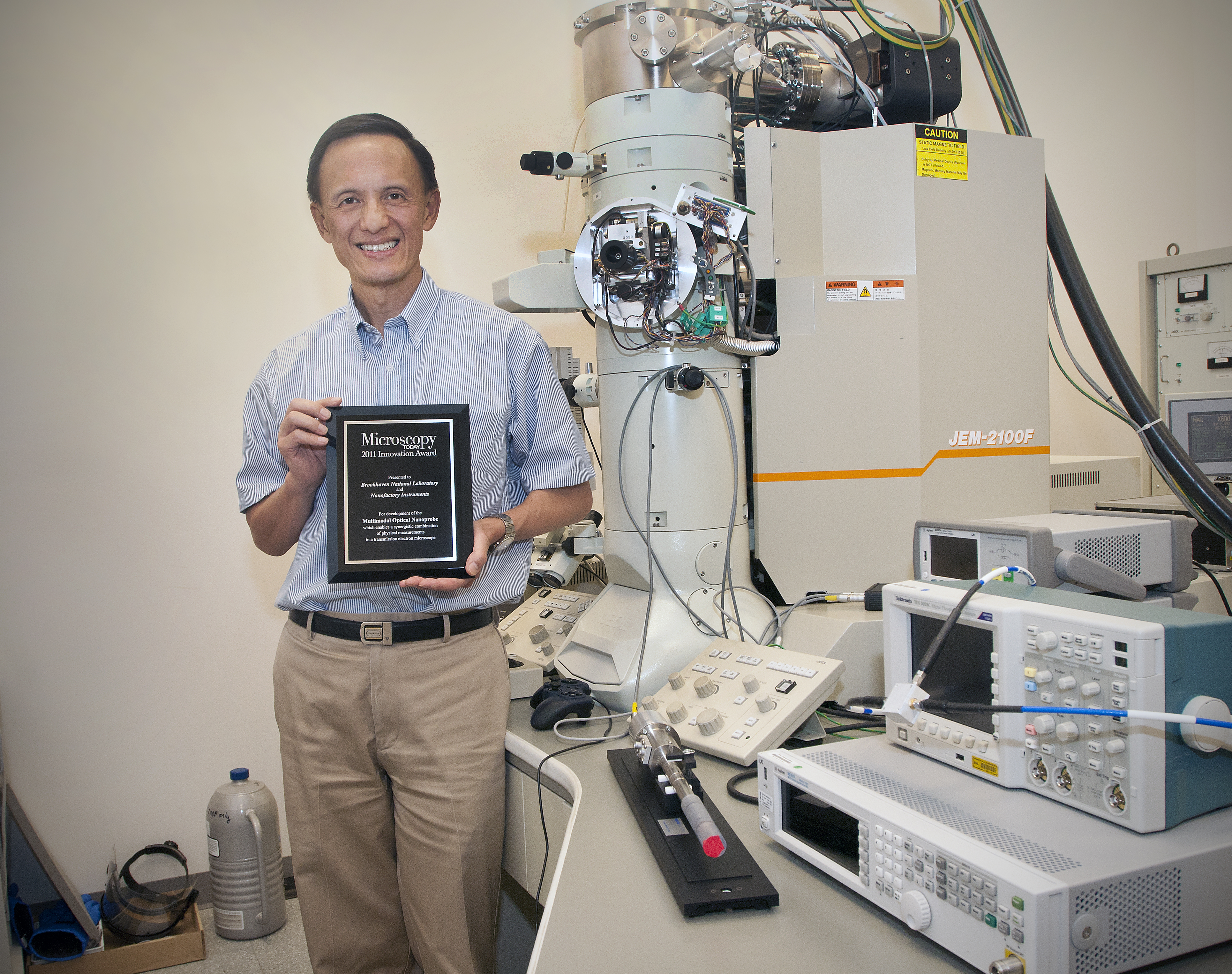
At the Microscopy Society of America’s annual meeting in Nashville, Tennessee, August 7-11, 2011, Brookhaven Lab senior physicist Yimei Zhu accepted the award on behalf of Brookhaven Lab and Nanofactory Instruments, AB. The award consists of a plaque that commends the institutions “for the development of the Multimodal Optical Nanoprobe which enables a synergistic combination of physical measurements in a Transmission Electron Microscope.”
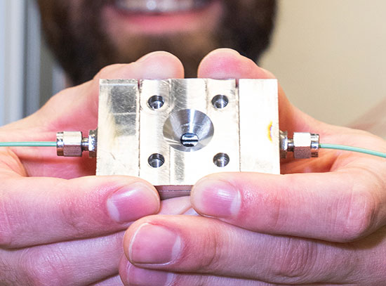
Zhu, a Brookhaven Lab senior physicist, led the Brookhaven team that worked with Nanofactory Instruments, AB, to develop the multimodal optical nanoprobe. The device is mounted on a transmission electron microscope to measure numerous properties of a sample simultaneously, in addition to imaging.
The nanoprobe measures the optical, electrical, mechanical, and structural properties of nano-sized materials and devices that are magnified from 1,000 to 50 million times. Combining various measurement techniques in one instrument offers a new level of material characterization that is not possible by sequential application of the techniques. These capabilities have been streamlined into a single package that, with minimal expense and difficulty, can be integrated into almost any electron microscopy system.
Zhu said, “The nanoprobe enables researchers to simultaneously measure a material’s structural behavior under various stimuli, including electric, optical, and mechanical ones, and to evaluate its functionality and performance. Here, simultaneously is the key. For example, if we want to improve the efficiency of a solar cell to harness energy for the sun, we need to shine a light on the device and measure the electric current it generates at same time, while observing the response of electronic structure and atomic arrangement at specific sites of interest. This capability is unprecedented and is a big improvement over sequentially determining these qualities.”
The nanoprobe can be used in a wide variety of experiments to help scientists understand how optical, electrical, mechanical, and structural properties of functional materials and devices are intertwined. This information is vital to making improvements in optoelectronic systems, such as fiber optic communications, laser systems, remote sensing systems, medical diagnostic systems, and optical information systems. It is an important tool in photovoltaics research to reveal site-specific optoelectronic properties of materials and devices. In other applications, the nanoprobe can help to determine strain effects on various properties of nanostructured materials, such as quantum dots, nanowires, and graphene sheets. The nanoprobe tip can be pressed on the point of interest in a sample to investigate the local stress response and strain distribution.
Brookhaven Lab designed and built the laser system and holder for the nanoprobe. Also, Brookhaven funded the construction of the device’s holder by Nanofactory Instruments, AB. In addition to Zhu, members of the Brookhaven team included Mirko Milas and Jonathan Rameau, both postdoctoral fellows; and Matt Sfeir, an assistant scientist. Brookhaven Science Associates, the company that manages Brookhaven Lab for the U.S. Department of Energy, has applied for a patent on the device. R&D Magazine chose the nanoprobe as one of the top 100 technological achievements of the year in 2011.
2011-11327 | INT/EXT | Newsroom