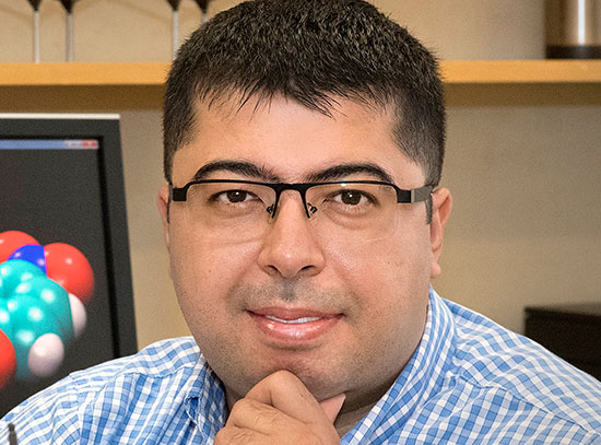
Q&A with CFN User Vinod Menon
Using the optical spectroscopy and microscopy capabilities at Brookhaven Lab's Center for Functional Nanomaterials (CFN), City College of New York Professor Menon studies light-matter interaction at extremely small scales
August 25, 2017
Vinod Menon
 Photonics—the science of using and manipulating photons, the smallest unit of light—touches nearly every aspect of our lives, from telecommunication and entertainment to medicine and homeland security. Vinod Menon, a physics professor at the City College of New York (CCNY) and the principal investigator at CCNY’s Laboratory for Nano and Micro Photonics, addresses fundamental questions related to how light behaves at the smallest possible dimensions. His research has brought him and his lab group to the Center for Functional Nanomaterials (CFN)—a U.S. Department of Energy Office of Science User Facility at Brookhaven National Laboratory—where they study light-matter interactions in micro- and nano-sized materials.
Why is light’s behavior at the microscale and nanoscale of interest?
At these size scales, light interacts differently with matter than it does at the macroscale. That is because the microscale and nanoscale have length scales comparable to the wavelength of visible light, which ranges from about 400 to 700 nanometers. In structures that are few nanometers in dimension, the length scales are much smaller than the wavelength of light.
Engineering materials with subwavelength structures opens up lots of opportunities to modify how light interacts with matter because light cannot “see” such structures since the wavelength of light is much larger. By designing materials with such structures, we can control and manipulate how light travels through matter, causing it to bounce around and become trapped, for instance, or even bending it in ways opposite of usual convention.
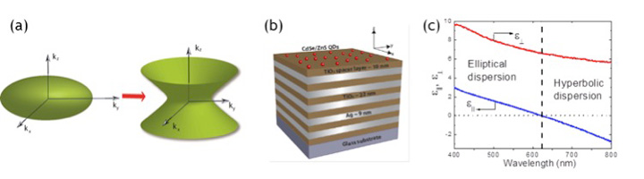
Menon led a team of physicists who created an artificial nanostructured material with layers of silver (Ag) and titanium dioxide (TiO2), as illustrated in (b). This material can be switched from a dielectric state (does not conduct electricity) to a medium that behaves like a metal in one direction and a dielectric in the other. The team uncovered an optical topological transition (c), or change in surface geometry, as depicted in (a), that results in a dramatic increase in the intensity of light inside the material and modification of the light-emission properties of tiny semiconductor quantum dots placed near the surface of the material. [Science, 2012]
What does research at the Laboratory for Nano and Micro Photonics focus on?
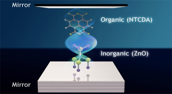
In 2014, while a professor at Queens College, Menon and his collaborators at the University of Michigan used light to bind together organic and inorganic semiconductors by sandwiching them between two mirrors that form a photon-trapping optical cavity. The combined matter demonstrates enhanced optical properties, such as light absorption, that could enable the development of more efficient solar cells and solid-state lighting. [Physical Review Letters, 2015]
After fabricating such materials, how do you study their structure and optical properties?
We use spectroscopy techniques to measure the amount of energy absorbed, reflected, or transmitted by a material after we shine a light beam on it. More often than not, we are interested in knowing the time dependence of the particular process being studied. Because these processes typically happen on extremely short timescales—nanoseconds or even tens or hundreds of picoseconds—we use lasers with ultrashort light pulses and high-speed detectors that can record the resulting spectral signals. If the optical response of a material is not a linear function of the intensity of the applied light source, which is usually a high-intensity laser, the material is said to be nonlinear. When the amount of light you put in is not proportional to the amount of light you get out, a number of effects can arise, such as a change in the material’s refractive index, or how quickly light travels through the material.
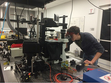
Student Charles Cohen looking into a confocal microscope at the Laboratory for Nano and Micro Photonics.
Why bring your research to the CFN?
Before coming to CCNY in 2014, I was at Queens College. Because Queens College is a small institution, I did not have access to state-of-the-art instrumentation needed to carry out ultrafast spectroscopy for my research. I also avoided projects that would require nanofabrication because Queens only had a small cleanroom with basic capabilities. Collaborating with someone who has access to the necessary tools is always an option, but that would mean the collaborator has to play a key role in the project. One of the problems in collaborating with another principal investigator is that my students would not get the hands-on training and experience that the investigator’s students would.
At CFN, my students learn ultrafast spectroscopy and nanofabrication techniques from CFN experts and perform all the measurements. Once I had access to CFN’s ultrafast spectroscopy tools, I soon realized there was also a fantastic nanofabrication facility there, and I started writing proposals for projects requiring nanofabrication. So CFN not only provided my group with access to state-of-art techniques for spectroscopy but also enabled us to expand our areas of research.
What CFN capabilities are critical to your lab’s research?
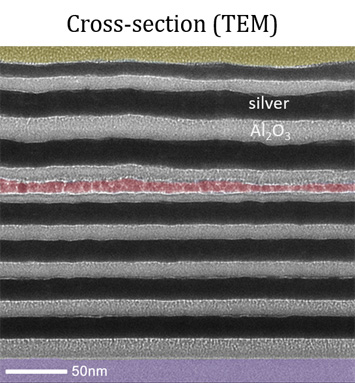
Transmission electron microscope (TEM) of cross section of smooth continuous films of silver and aluminum oxide.
 enlarge
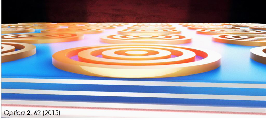
Menon and his group designed a bulls-eye grating structure and deposited it on top of a material they engineered based on their silver-germanium-aluminum oxide layering scheme, with quantum dots embedded in one of the aluminum oxide layers. With this material, they not only demonstrated an increase in light emission but also were able to extract light. [Optica, 2015]
At the peak of our usage, we were using all three CFN facilities. Now, most of the time, we are using CFN’s really unique optical spectroscopy and microscopy capabilities that enable us to get time-resolved measurements and images showing intensity patterns. The very fast timescales of the processes we are interested in would not be easily studied with standard off-the-shelf instruments.
Recently, we relied on these capabilities to look at the light-emission properties in a new class of artificial materials called photonic hypercrystals, which combine the properties of light-manipulating photonic crystals (periodic nanostructures) and metamaterials (engineered materials with properties not found in nature). In our photonic hypercrystals, the metamaterial is based on the silver-germanium-aluminum oxide layering scheme we imaged at CFN. Semiconductor nanoparticles (quantum dots) embedded in one of the metamaterial layers quickly emit visible light. The photonic crystals are subwavelength holes milled into the top two silver layers. Because of their periodicity, these holes efficiently scatter light.
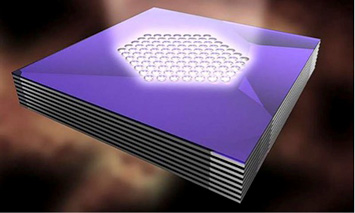
An illustration of a photonic hypercrystal. [Proceedings of the National Academy of Sciences, 2017]
How has the expertise of the CFN research community impacted your research?
The CFN research community has played an important role, especially for my students. Every one of them went into CFN with zero experience in any of the nanofabrication and optics techniques and came out as experts. They have gone on to attain positions at universities and government labs, including UC Berkeley, the National University of Singapore, and the Air Force Research Laboratory, and the last student who graduated was just chosen as a finalist for a thesis award given by the American Physical Society.
My research group has also collaborated with CFN scientists. Working with physicist Matt Sfeir, who is the point of contact for the ultrafast and nonlinear spectroscopy instruments at CFN, we studied random lasing in powders of the semiconductor zinc oxide (ZnO). Typically for a laser you need an optical cavity that confines light, but in certain disordered materials like powders, light scattering between particles can cause light to reflect back to its initial position, forming closed loops that act as laser cavities and amplify the light. We demonstrated random lasing in subwavelength thin films of highly crystalline ZnO nanospheres. Lasing in such a thin film of ZnO is important because it could lead to the development of low-cost, low-power, high-efficiency photonic devices like solar cells.
What are some of the projects you are currently working on?
We are working toward a real design for building an ultrafast LED; looking at the coupling of excitons (excited state consisting of bound electron-hole pairs) with light in a new class of semiconductors that are only a few atomic layers thick; developing new material platforms for realizing single-photon emitters, which are a necessary building block for quantum information processing; and investigating simplistic experimental models to see if cooperative effects between molecules can enhance energy transfer in hybrid organic-inorganic nanomaterials. We are also starting to investigate the modification of molecular transitions and chemical reaction pathways through coupling of molecular excitations to light-trapping structures.
Photonics is already embedded in our lives, but how do you see it advancing?
I see a lot of potential in multiple areas. Medicine is already seeing progress in using photonics for imaging during surgery, and optical and photonics technologies are advancing entertainment display systems like virtual and augmented reality headsets. Though solar cells have been around for some time, photonics has been having a larger contribution lately because it is not enough to have solar cell materials that absorb light efficiently. We need materials that can efficiently manage the light, trapping it or slowing it down, for instance.
 enlarge
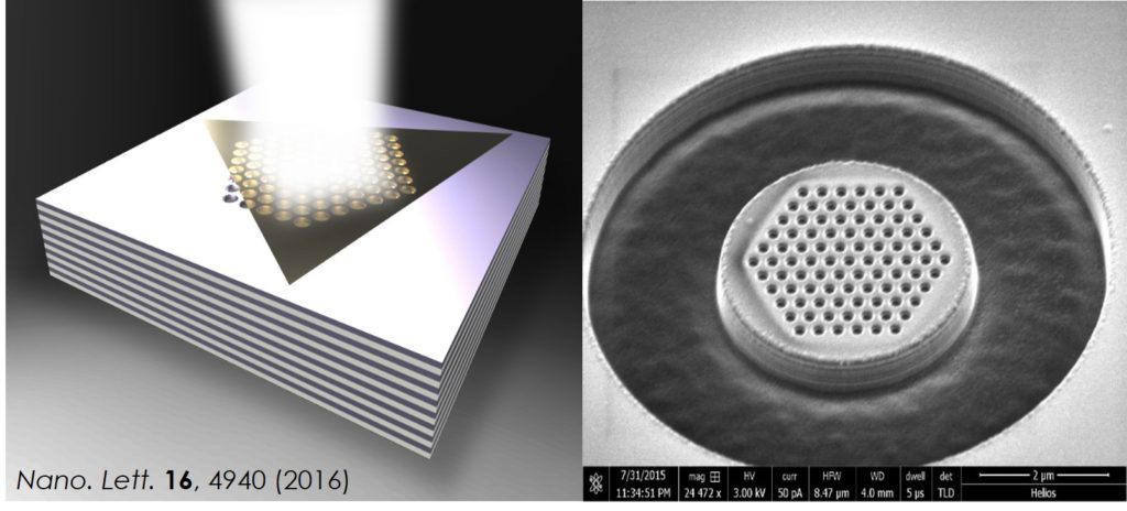
Menon's team placed two-dimensional materials called transition metal dichalcogenides (TMDs) on top of a photonic hypercrystal, as illustrated on the left. The scanning electron microscope image on the right shows the photonic hypercrystal etched from a metamaterial. TMDs have electronic and optical properties, such as spontaneous light emission, that make them of interest for future optoelectronic devices. However, they do not currently emit enough light to be practical for such devices. The photonic hypercrystals make the TMDs much brighter sources of light. [Nano Letters, 2016]
New areas include ultrafast LEDs for LiFi, which could overcome the bottlenecks of today’s wireless communication, and for signal processing and computing. I truly believe the photon is the best carrier of quantum information, though it might not be the best processor. Single-photon (quantum bit) generation and manipulation is going to be the next big wave of photonic applications. Quantum computers hold the power to perform calculations much quicker, solve problems beyond the reach of regular (classical) computers, and send information much more securely.
Do you participate in any activities outside your day-to-day responsibilities?
I am actively involved in outreach activities. Each summer, I host high school students in my lab. This year, I have five students. A graduate student or postdoc works closely with each of them, and I try to spend as much time with them as I can. In addition to doing hands-on characterizations and simulations using tools we developed, the students receive physics lessons, participate in our group meetings, and learn how to make a scientific presentation. At the end of the summer, they present their projects and write a short report. Many of my former students have won prizes at national science fairs. I also have high school students from the Harlem area come see what we do in the lab, hopefully piquing their interest in science.
By far, my biggest outreach effort has been my appearances on Science Goes to the Movies, a series hosted by the City University of New York (CUNY) that explores the science featured in films and popular TV shows. In one episode, I explained how light is used in films including Star Wars, Star Trek, and Fantastic Four—lightsabers, tractor beams, and so on. In a more recent episode, I discussed holograms as depicted in Iron Man, Star Wars, and Star Trek and talked about my experience using the Microsoft HoloLens, a holographic computer and head-mounted display. These episodes are now airing on PBS.
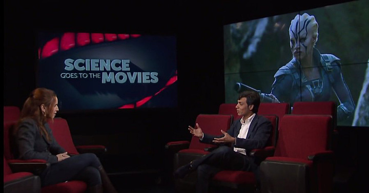
Vinod Menon talks with CUNY's Science Goes to the Movies host Faith Salie about the method that Star Trek character Jaylah uses to create holograms and explains how holograms are really made.
How did you become interested in science in general and photonics in particular?
I wanted to be a scientist for a really long time. I grew up in India—a place where science is highly valued and everyone wants to become an engineer or a doctor. As someone who had always been interested in basic science, I was a slight deviant in that sense.
Before high school, I was drawn toward robotics and artificial intelligence. At the time, someone in my family was attending grad school in the field, so that definitely contributed to my interest. My interest shifted to physics in high school, when I started reading more popular science books and watching popular science TV shows. I realized that, as long as I understood the concepts in physics, I did not need to memorize much in order to solve problems. My love for physics is rooted in my desire to understand how nature behaves and use concepts from nature in new areas.
Light had always been something I was fascinated by. India has always had a strong tradition in optics. My interest was solidified when I completed my master’s degree in physics at the University of Hyderabad, India, which has a specialization in quantum optics. At this point, I was not sure if I wanted to do theory or experiment; I was open to both. After spending a summer in an experimental lab, I knew I wanted to be an experimentalist. I came to the United States to continue my studies at the University of Massachusetts–Lowell, where I received my PhD in physics. I then did postdoctoral work in integrated photonics at Princeton University, mostly making optical chips that do logic and signal processing functions—optical analogs of electronic chips. Moving on to my own independent group at CUNY as part of the Photonics Initiative, I started exploring both fundamental and applied questions pertaining to the interaction of light with matter. I have been lucky to have some fantastic students and post docs, and my group is one of the things that keeps me going and something I am very proud of!
Brookhaven National Laboratory is supported by the Office of Science of the U.S. Department of Energy. The Office of Science is the single largest supporter of basic research in the physical sciences in the United States, and is working to address some of the most pressing challenges of our time. For more information, please visit science.energy.gov.
2017-12328 | INT/EXT | Newsroom