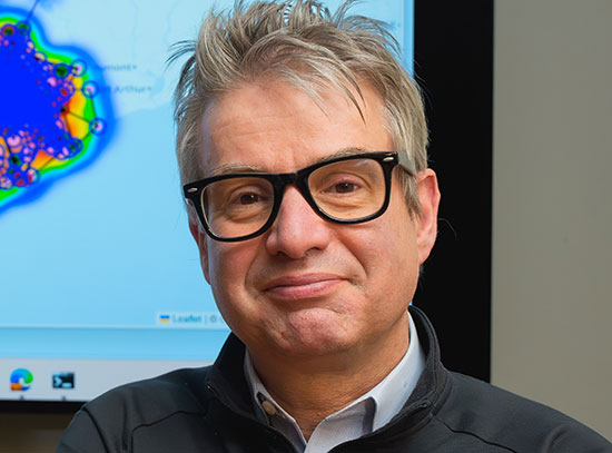
Meet Longtime IBM/Brookhaven Lab Scientist Jean Jordan-Sweet
Jordan-Sweet retired after a nearly 40-year career based at Brookhaven Lab
December 1, 2021
 enlarge
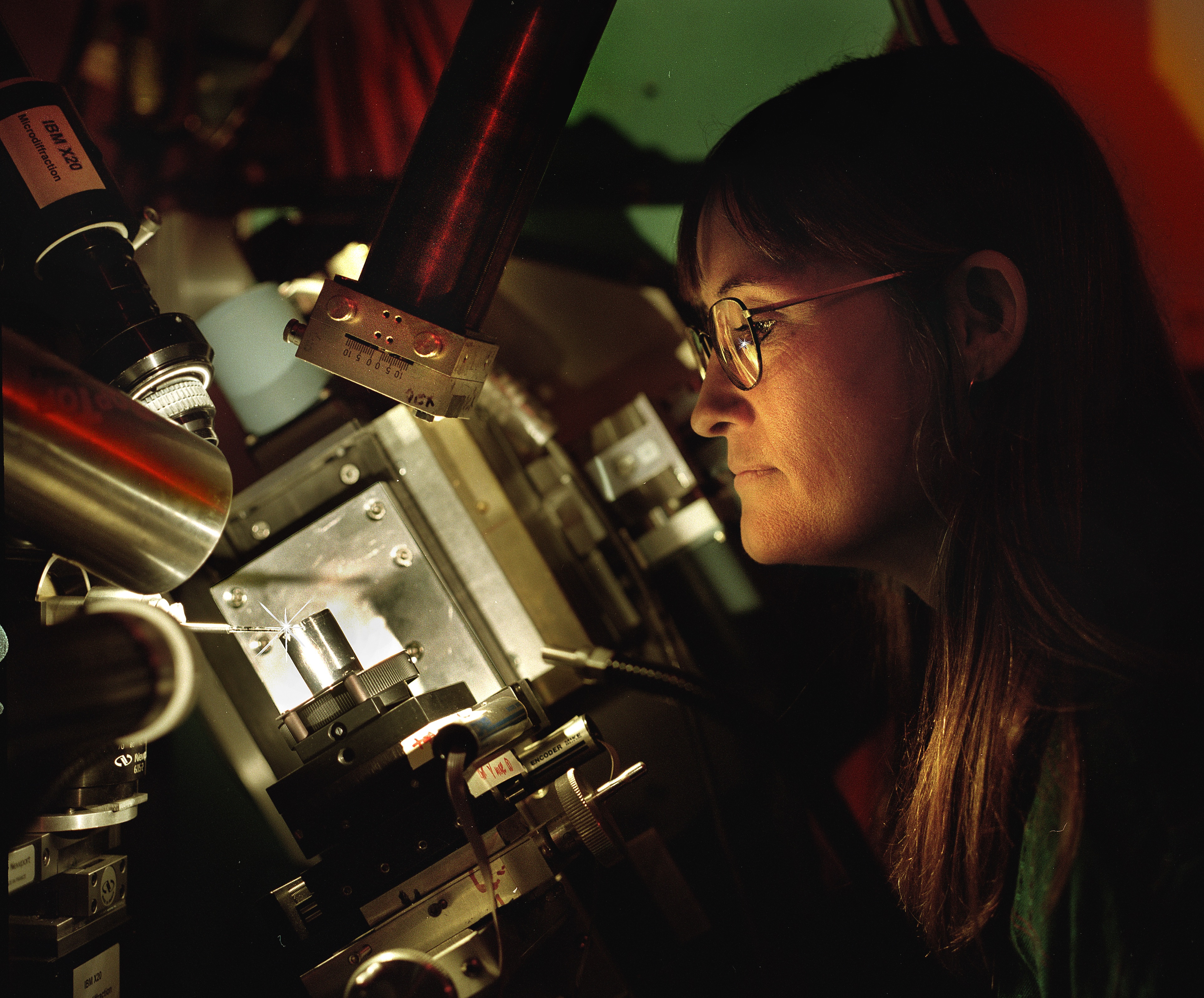
This photo shows Jean Jordan-Sweet with the microbeam setup at beamline X20A at NSLS in 2001.
Prior to her retirement in August, Jean Jordan-Sweet was a senior engineer at IBM Research and a beamline scientist at the Beamline for Materials Measurement at National Synchrotron Light Source II (NSLS-II), a U.S. Department of Energy (DOE) User Facility located at DOE’s Brookhaven National Laboratory. For almost 40 years, her work has focused on using x-ray techniques to study materials and processes for the advancement of microelectronics technologies.
What brought you to Brookhaven Lab at the start of your career?
I first came to Brookhaven Lab about 40 years ago as a grad student from the University of California at Los Angeles (UCLA) and did some of my thesis experiments here.
 enlarge
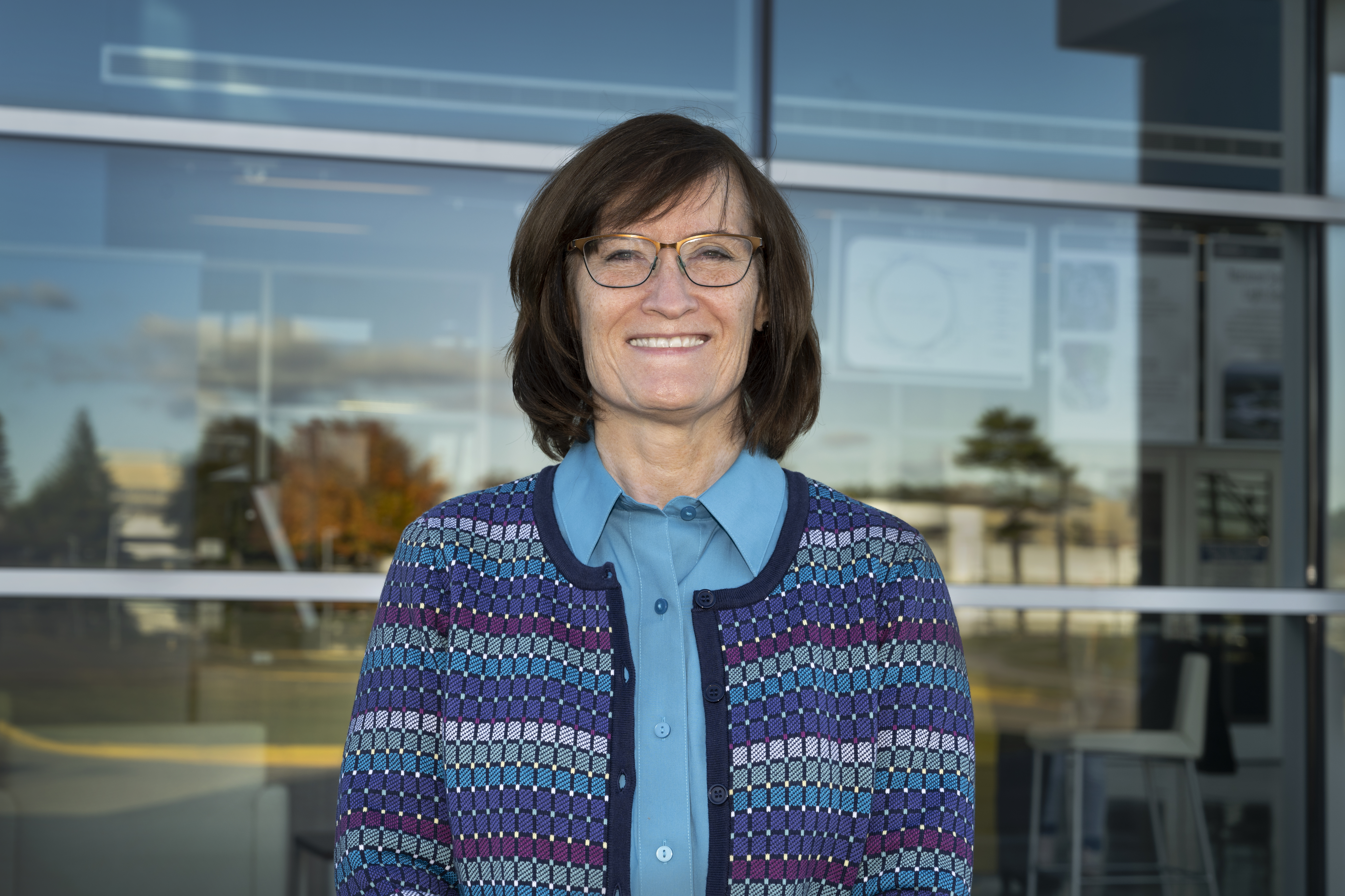
Jean Jordan-Sweet is looking forward to continue working with the National Institute of Standards and Technology (NIST) at NSLS-II after her departure from IBM in 2021.
My advisor at UCLA, John McTague, had been a collaborator on a project using x-rays at early synchrotrons to look at adsorbed inert gas films, which form two dimensional phases. At that time, the brightness of x-rays wasn’t good enough to look at a single surface the way we can now, so we had to make substrates that were in powder form. Using a powder meant having a lot of small crystals that together had enough surface area to get a signal from the adsorbed film. My thesis involved making a high-surface-area powder substrate that had a special symmetry. So, I made magnesium oxide (MgO) powder, which has square surface symmetry. I used a rotating anode x-ray source at Brookhaven to study the two-dimensional melting of krypton adsorbed on MgO. That source was owned by Dave Moncton, who was a collaborator with my advisor. I used that instrument 24/7 for a couple of weeks to take my thesis data.
We also collaborated with Larry Passell, who was my mentor here at Brookhaven Lab and part of the Condensed Matter Physics Department. He is a wonderful man and I enjoy visiting him to this day. I analyzed all my thesis data with his help and graduated in 1983. I then got a postdoc with IBM on the ultraviolet (UV) section of the National Synchrotron Light Source (NSLS), the predecessor of NSLS-II. I started out by studying polymer/metal interfaces using UV spectroscopy. From there, it was a natural progression to apply for a job to run IBM’s x-ray diffraction beamlines at NSLS. In 1986, I was hired by IBM permanently to do just that.
What was your work like in those early years at NSLS?
In the late 80s, industry claimed a large fraction of NSLS beamlines; there were Exxon, Bell Labs, and Dow/Dupont, for example. IBM had about seven beamlines at NSLS, and they all did different things. A couple did x-ray lithography, two were for x-ray diffraction, and there was a suite of beamlines for optics development and ultraviolet spectroscopy.
IBM originally entered into a partner-oriented operational mode at NSLS, mainly to be able to control what kind of instrumentation we developed and had access to. We were collaborating with scientists at the Massachusetts Institute of Technology (MIT), where they did a lot of condensed matter physics research and IBM did a lot of microelectronics-related research. Back then it was relatively inexpensive to put a beamline together. We operated the X20 diffraction beamlines until the end of NSLS.
What scientific questions drove your research?
In the early days of my career, IBM was a very vertically-integrated company. They did everything, from making the chips to building the displays and the hard drives. They were just starting to make PCs at that time. So, there were a lot of different materials to study with x-rays, such as the orientation of the liquid crystals used in flat-panel displays, and the component materials that make up microprocessors and storage devices.
 enlarge
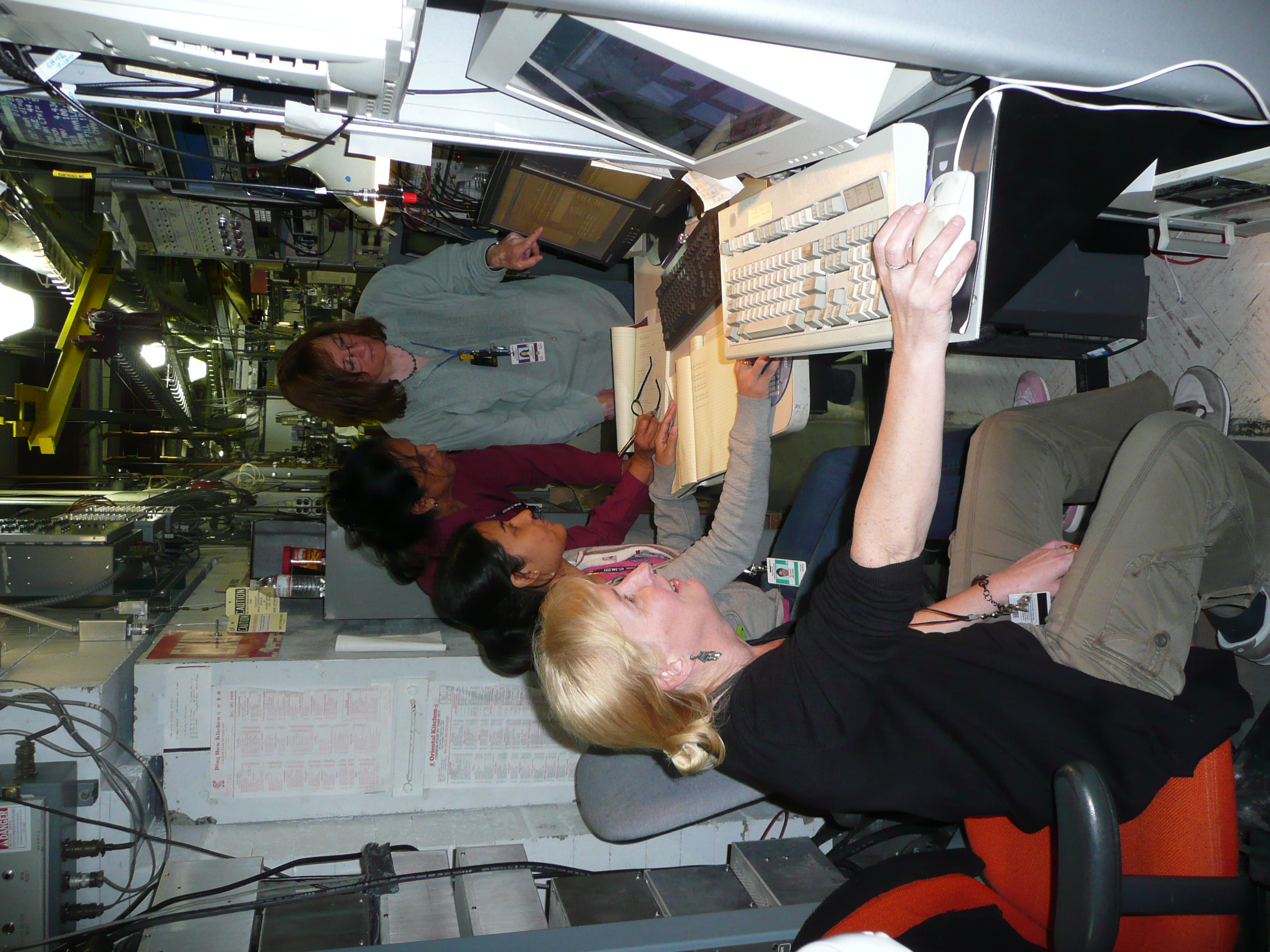
Jean Jordan-Sweet (in the back) with three other researchers shown here taking data at the X20C beamline at NSLS. Image courtesy of Jean Jordan-Sweet.
A lot of the measurements we took were aimed at understanding the behavior and characteristics of thin films or stacks of thin films. When you make a chip, it’s got hundreds of different layers. Every layer is deposited and processed according to some recipe, whether it’s implanted, annealed and/or etched. So, there are many different materials and processes to study. We could use x-rays to do all sorts of measurements.
Currently, IBM is concentrating on very advanced computation like artificial intelligence (AI), neuromorphic computing, and quantum computing, so they develop very high-end hardware. IBM is looking at entirely different ways of doing computation, such as using memory as a computing device for AI. These approaches are more analog than digital because you are trying to mimic the synaptic pathways of a brain. Those architectures involve a whole different set of materials.
Then there is quantum computing. That hardware is completely different and involves another set of materials operating at ultra-low temperatures. We have almost the whole periodic table to play with.
How did you become interested in this work?
In high school, I had a very good physics teacher, and he got me thinking about a career in science. Then in college, I double-majored in physics and chemistry. I also did a couple of National Science Foundation summer programs: One when I was a junior in high school, and the other when I was a junior in college. The one during college was at Argonne National Laboratory. I was taking a tour of Chicago Pile-5, which was the last version of their nuclear reactor for science research. I was looking around at the size of the instruments and all the neat stuff; it was like a beehive in there. And I thought, wow, it would be so cool to work at a place like this.
What have you been working on recently?
Prior to my retirement, I worked at the Beamline for Materials Measurements, also called BMM, which is led by Bruce Ravel, and we signed a CRADA with the National Institute of Standards and Technology (NIST) to put an x-ray diffraction end station in the downstream end of Bruce’s hutch. IBM gets about one-sixth of the beamtime for experiments, where we do mostly diffraction and x-ray reflectivity. We also have used the spectroscopy capabilities to help us explore samples not easily characterized with x-ray diffraction.
BMM is a fantastic source for us. Bruce has it so well programmed; I never have to calibrate the energy and it practically aligns itself. It’s been a pleasure working there. The source at NSLS-II is so stable, with a constant beam intensity, that it’s much easier to do experiments here than at NSLS.
A paper that we published this year was about trying to understand the crystal structure of thin hafnium oxide films that have been doped to become ferroelectric. This material is a candidate for another sort of memory — ferroelectric memory — that is being developed for neuromorphic computing. Nobody had yet definitively determined the structure of the ferroelectric phase. Oxides like these have peaks all over the place on an x-ray diffraction plot and it’s really hard to pin down what the structure is. At BMM, along with colleagues from IBM, NIST, and Seton Hall University, we used x-ray absorption spectroscopy at NSLS-II and density functional theory modelling to really pin down the structure of that ferroelectric phase. We nailed it and published a paper in Applied Physics Letters.
What are some highlights of your career?
I think, for IBM, our most impactful development was the thermal annealing x-ray diffraction system, which is a highly specialized chamber mounted on a diffractometer. Thermal processing of layers is one of the most common steps in chip manufacturing. In our system, thin film or patterned samples on wafer pieces are clamped onto a heater using what is called a four-point probe, which measures electrical resistance in a film. X-rays diffract from the film onto a linear detector while the sample is being quickly heated to a desired temperature. We also had a laser that would reflect off the surface and scatter, and the intensity of the scattered light would tell you how rough the surface was on several length scales. This comprehensive system allowed us to measure temperature and kinetics of phase formation or crystallization depending on a large number of variables, such as dopants added, deposition method, substrate used, etc.
 enlarge
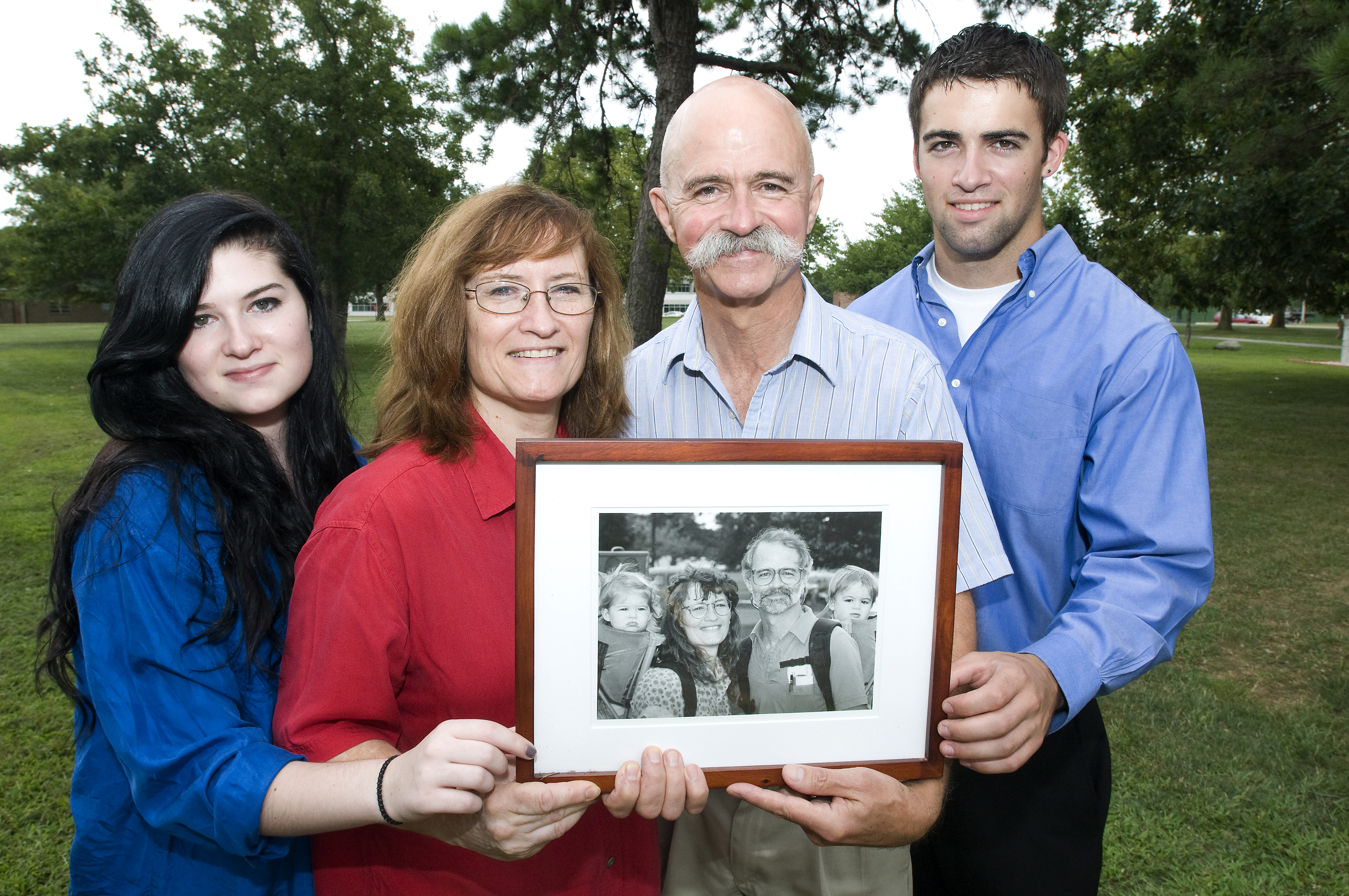
Brookhaven Lab is a family affair for the Sweets, as shown in this photo of Alan, Jean, Bob, and Marie taken during a poster session of Brookhaven's summer intern program in 2011, while they're holding a photo taken at the 45th Brookhaven Lab anniversary picnic in 1994. Bob works in the structural biology program at NSLS-II.
We used that technique to look at the formation of the little contact pads that are part of the wiring on a computer chip; they are called self-aligned silicides and are formed by reacting metal with the underlying semiconducting areas that form the transistor gate, source, and drain. It is important that these contacts have very low resistance because you are bringing a low voltage signal in and out. Over the years we studied tons of metal films on different semiconductors, creating a giant database of what structures were formed under various conditions — 35,000 data runs in total.
During the last years of NSLS operations, when IBM was using nickel silicide as a contact pad, they found out that their manufacturing yield for a new processor chip was terrible. A big mass of nickel silicide (NiSi) sometimes formed right in the carrier channel and shorted out the transistors. It was called the “NiSi fang defect” because it was shaped like a fang. We pinpointed the cause by looking at the geometry of the device, referring to our enormous database, and doing some additional measurements on our instrument. The problem was solved by adding a second annealing step that converted some Ni-rich silicide created during an etching step back to NiSi. IBM had been facing a months-long delay in the sale of a new generation of servers and avoiding that was a big deal.
We received an IBM Research Outstanding Technical Achievement award for that, which is hanging on my wall.
What was it like to navigate the end of NSLS and the beginning of NSLS-II?
The gap between NSLS and NSLS-II was tough. It was a crazy time. We did some runs as general users at other synchrotrons. But I had to take apart our old X20 beamlines, figure out who to donate stuff to, clean it up, crate it, and ship it out. It took a year to get all that done. We shipped out almost 15 tons of equipment! And at that time, right before the NSLS shut down, we also had built and commissioned an automated annealing/x-ray diffraction end station that was sent up to the Canadian Light Source. That also had to be crated and shipped out.
“Last light” at NSLS was tough. Some managers came down from IBM, as well as some of our collaborators, and it was really nice that they wanted to witness it. I was actually taking a measurement there at the very end. It’s called a pole figure, which is a way to measure microcrystalline film texture. It took two and a half hours to do this, it was a whole series of scans. I remember watching the clock tick down. The experiment finished about 30 seconds before they did the final beam dump.
Did you enjoy your years at the Brookhaven Lab’s light sources?
Overall, very much so. The staff is great, my collaborators have been fantastic. I’ve been so impressed over the years with how smart the people are who come here and the amazing projects they work on.
I’ve been very lucky, because what is the likelihood of industry supporting someone working at a national lab for 37 years? It’s been a good run! I appreciate that IBM has recognized the value of this research and provided for me to stay here for my whole career.
What is next for you?
I’m hoping that I can still keep my foot in the door. In February, we brought in Vesna Stanic to take my place running the IBM end station at NSLS-II, and she is very good at that. She has loads of synchrotron experience, but she’s still not completely familiar with all of the instrumentation that I put together. We’ve only done three runs together since she arrived. So, I would like to make sure that the transition continues and that I can come in to help set up for users or when there is an equipment upgrade.
In our CRADA renewal, we’re proposing to develop more varied sample environments. Our diffractometer doesn’t have a big volume where the sample sits. We want to develop and build some temperature variation capabilities via a heating stage and hopefully a cooling stage. I hope to be involved in this.
And recently, we have been developing a translation mechanism so that we can study combinatorial samples. You can have a wafer with all sorts of variations in processing, like gradients from annealing or co-deposition, for example. I installed one linear stage last year and I’m putting in the second one now. They are a big aid for remote access users. Being able to study combinatorial samples is also an important application for machine learning, which is a current focus of IBM as well as Brookhaven Lab.
In the near term, I will be an associate of NIST, which allows me to work at BMM, only my affiliation has switched to NIST. I hope to continue at Brookhaven Lab in this way.
But in the meantime, I have some plans. I took a big family canoeing trip up to the Boundary Waters region at the U.S/Canada border in August and will be doing more travel to visit family and friends. I also like to make stained glass and other craft-oriented art. I have a friend in Wading River, a physicist recently retired from Brookhaven Lab, who is an excellent woodworker and has a really creative, artistic imagination. We want to collaborate on some projects. I also like to go birding, and my younger sister and I would love to go to Texas to see painted buntings, which is on our bucket lists.
As a U.S. Department of Energy Office of Science User Facility, NSLS-II enables a collaborative, holistic approach to advance scientific endeavors by offering free access to highly advanced instruments and unique expertise. To learn more about research capabilities and collaborations with NSLS-II staff, please visit the NSLS-II website.
Brookhaven National Laboratory is supported by the U.S. Department of Energy’s Office of Science. The Office of Science is the single largest supporter of basic research in the physical sciences in the United States and is working to address some of the most pressing challenges of our time. For more information, visit https://energy.gov/science.
Follow @BrookhavenLab on Twitter or find us on Facebook.
2021-19268 | INT/EXT | Newsroom