Seeing Inside Next-Generation Microelectronics Using X-rays
Scientists used non-destructive x-ray mapping to understand the deformation in novel gate-all-around structures
August 10, 2022
 enlarge
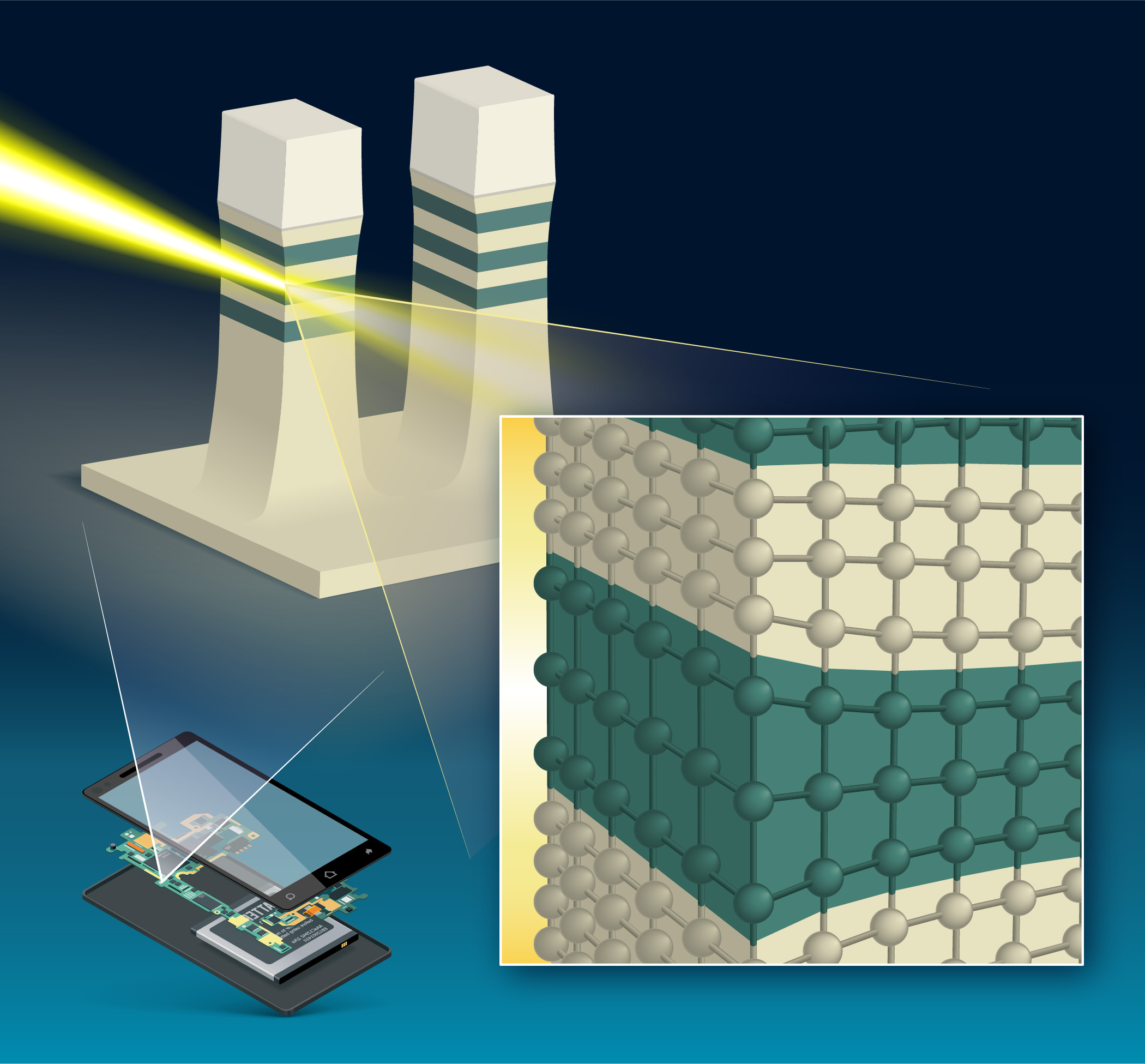
This artist's impression shows how x-rays made it possible to study the distortions of the layers in the material. The atoms at the edges of the layers are either squished tighter or pulled apart, creating a bend along the different layers. (Image courtesy of Brookhaven National Laboratory)
The Science
Scientists found two competing mechanisms that contribute to the deformation of nanosheets, which are novel structures employed for next-generation Gate-All-Around Field Effect Transistors (GAAFETs), by using non-destructive x-ray diffraction mapping with 12 nanometer (nm) resolution.
The Impact
The performance of next-generation nanoelectronic devices relies on the precise understanding of their inner structure, which can only be achieved if researchers can visualize the deformations of these materials using a non-destructive method.
Summary
The demand for ever smaller electronic devices requires researchers to design devices using novel nanoscale geometrics with complex fabrication processes. While technological advances made these developments possible, understanding the essential inner details, such as deformation, of these tiny devices—in a way that doesn’t destroy the initial structure—has become exceedingly difficult.
In this study, a team of researchers from IBM collaborated with scientists from the National Synchrotron Light Source II (NSLS-II) to map the deformations within nanosheets, novel structures employed for GAAFETs, using the Hard X-ray Nanoprobe (HXN) beamline. By exploiting the brilliant source of NSLS-II and the resolving power provided by in-house developed nanofocusing optics called a multilayer Laue lens, they were able to identify two competing mechanisms at different length scales that contribute to the deformation. The first, which is long-range and previously known, is due to the mismatch of lattice constants between the different elements and a relaxation effect near the edges. The second, a much shorter-range effect, is associated with the layering itself and is dominant is dominant at the edge of the layer within a length scale equivalent to the nanosheet's thickness. These new insights could help them predict essential performance parameters such as the carrier mobility of future devices.
Download the research summary slide (PDF)
Contact
Conal E. Murrray
IBM T.J. Watson Research Center,
conal@us.ibm.com
Hanfei Yan
National Synchrotron Light Source II, Brookhaven National Laboratory
hyan@bnl.gov
Publications
C.E. Murray, H. Yan, C. Lavoie, J. Jordan-Sweet, A. Pattammattel, K. Reuter, M. Hasanuzzaman, N. Lanzillo, R. Robison, N. Loubet. Mapping of the mechanical response in Si/SiGe nanosheet device geometries. Nature Communications Engineering 1, 11 (2022)
Funding
This research used 3ID beamlines of the National Synchrotron Light Source II, a U.S. Department of Energy (DOE) Office of Science User Facility operated for the DOE Office of Science by Brookhaven National Laboratory under Contract No. DE-SC0012704.
2022-20883 | INT/EXT | Newsroom