Researchers Image Electron Clouds on the Surface of Graphene, Revealing How Folds in the Remarkable Material Can Harm Conductivity
June 28, 2011
The following news release is being distributed by the University of Buffalo about work conducted, in part, at the National Synchrotron Light Source.
 enlarge
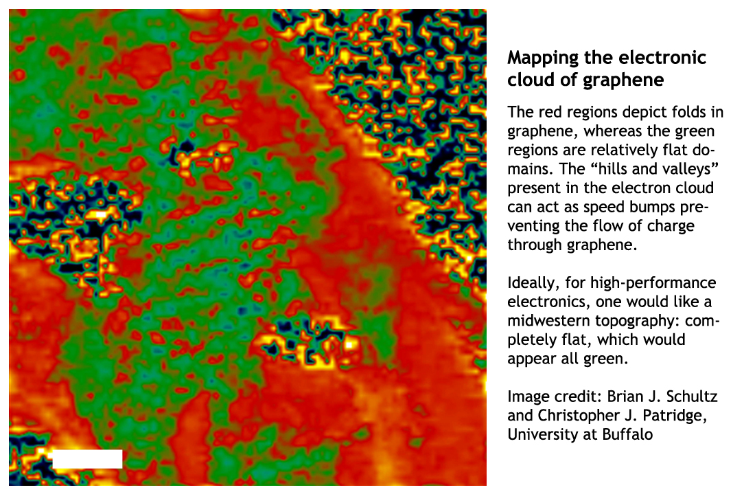
Mapping the electronic cloud of graphene
The red regions depict folds in graphene, whereas the green regions are relatively flat domains. The "hills and valleys" present in the electron cloud can act as speed bumps preventing the flow of charge through graphene.
Ideally, for high-performance electronics, one would like a midwestern topography: completely flat, which would appear all green.
Image credit: Brian J. Schultz and Christopher J. Patridge, University at Buffalo
BUFFALO, N.Y. — A research team led by University at Buffalo chemists has used synchrotron light sources to observe the electron clouds on the surface of graphene, producing a series of images that reveal how folds and ripples in the remarkable material can harm its conductivity.
The research, scheduled to appear June 28 in Nature Communications, was conducted by UB, the National Institute of Standards and Technology (NIST), the Molecular Foundry at Lawrence Berkeley National Laboratory (Berkeley Lab), and SEMATECH, a global consortium of semiconductor manufacturers.
Graphene, the thinnest and strongest material known to man, consists of a single layer of carbon atoms linked in a honeycomb-like arrangement.
Graphene's special structure makes it incredibly conductive: Under ideal circumstances, when graphene is completely flat, electric charges speed through it without encountering many obstacles, said Sarbajit Banerjee, one of the UB researchers who led the study in Nature Communications.
But conditions are not always optimal.
The new images that Banerjee and his colleagues captured show that when graphene is folded or bent, the electron cloud lining its surface also becomes warped, making it more difficult for an electric charge to travel through.
"When graphene is flat, things just kind of coast along the cloud. They don't have to hop across anything. It's like a superhighway," said Banerjee, an assistant professor of chemistry. "But if you bend it, now there are some obstacles; imagine the difference between a freshly paved highway and one with construction work along the length forcing lane changes.
"When we imaged the electron cloud, you can imagine this big fluffy pillow, and we saw that the pillow is bent here and there," said Banerjee, whose National Science Foundation CAREER award provided the primary funding for the project.
 enlarge
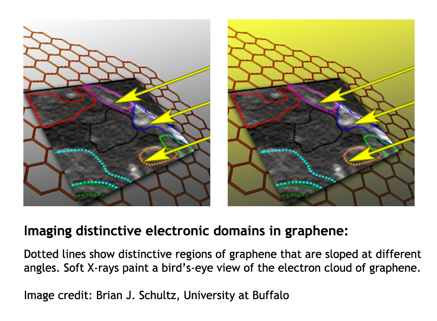
Imaging distinctive electronic domains in graphene:
Dotted lines show distinctive regions of graphene that are sloped at different angles. Soft X-rays paint a bird's-eye view of the electron cloud of graphene.
Image credit: Brian J. Schultz, University at Buffalo
To create the images and understand the factors perturbing the electron cloud, Banerjee and his partners employed two techniques that required use of a synchrotron: scanning transmission x-ray microscopy and near edge x-ray absorption fine structure (NEXAFS), a type of absorption spectroscopy. The experiments were further supported by computer simulations performed on computing clusters at Berkeley Lab.
"Using simulations, we can better understand the measurements our colleagues made using x-rays, and better predict how subtle changes in the structure of graphene affect its electronic properties," said David Prendergast, a staff scientist in the Theory of Nanostructures Facility at the Molecular Foundry at Berkeley Lab.
"We saw that regions of graphene were sloped at different angles, like looking down onto the slanted roofs of many houses packed close together."
Besides documenting how folds in graphene distort its electron cloud, the research team discovered that contaminants that cling to graphene during processing linger in valleys where the material is uneven. Such contaminants uniquely distort the electron cloud, changing the strength with which the cloud is bound to the underlying atoms.
Graphene's unusual properties have generated excitement in industries including computing, energy and defense. Scientists say that graphene's electrical conductivity matches that of copper, and that graphene's thermal conductivity is the best of any known material.
But the new, UB-led study suggests that companies hoping to incorporate graphene into products such as conductive inks, ultrafast transistors and solar panels could benefit from more basic research on the nanomaterial. Improved processes for transferring flat sheets of graphene onto commercial products could greatly increase those products' efficiency.
"A lot of people know how to grow graphene, but it's not well understood how to transfer it onto something without it folding onto itself," Banerjee said. "It's very hard to keep straight and flat, and our work is really bringing home the point of why that's so important."
"Graphene is going to be very important in electronics," said PhD candidate Brian Schultz, one of three UB graduate students who were lead authors on the Nature Communications paper. "It's going to be one of the most conductive materials ever found, and it has the capability to be used as an ultrahigh-frequency transistor or as a possible replacement for silicon chips, the backbone of current commercial electronics.
"When graphene was discovered, people were just so excited that it was such a good material that people really wanted to go with it and run as fast as possible," Schultz continued. "But what we're showing is that you really have to do some fundamental research before you understand how to process it and how to get it into electronics."
Other research partners offered the following insight into the significance of the findings:
— Dan Fischer, NIST Material Measurement Laboratory, leader, Synchrotron Methods Group: "The NEXAFS results indicating that performance-damaging contaminants cling to graphene during processing highlights the importance of chemically sensitive advanced synchrotron measurement method developments for promoting innovation and industrial competiveness in commercial applications of nanotechnology."
— Pat Lysaght, SEMATECH Front End Processes, senior member technical staff: "We place a premium on the power of collaboration, and this is a great example of the benefits associated with that philosophy. The unique expertise of each of the four collaborative entities has come together to forge a new understanding of subtle functionalization variations of surface graphene atoms. Our findings represent another important step toward potential industrial applications such as low-cost broadband radio frequency (RF) devices, and correlation of NEXAFS with Raman spectroscopy which may enhance monitoring capabilities for graphene as a replacement for large area organic LED displays."
Synchrotron imaging was conducted at the Canadian Light Source in Saskatchewan in Canada and at the National Synchrotron Light Source (NSLS) at Brookhaven National Laboratory in New York State. NEXAFS was measured at the NIST soft X-ray beamline of the NSLS.
Portions of this work conducted at the Molecular Foundry were supported by the Department of Energy Office of Science. The Molecular Foundry is one of five DOE Nanoscale Science Research Centers (NSRCs), premier national user facilities for interdisciplinary research at the nanoscale. Together the NSRCs comprise a suite of complementary facilities that provide researchers with state-of-the-art capabilities to fabricate, process, characterize and model nanoscale materials, and constitute the largest infrastructure investment of the National Nanotechnology Initiative.
Additional support for the project came from a New York State Energy Research and Development Authority (NYSERDA) grant disbursed through Graphene Devices, a Western New York start-up company exploring ways to optimize production of graphene using processes that Banerjee and UB colleagues invented.
The University at Buffalo is a premier research-intensive public university, a flagship institution in the State University of New York system and its largest and most comprehensive campus. UB's more than 28,000 students pursue their academic interests through more than 300 undergraduate, graduate and professional degree programs. Founded in 1846, the University at Buffalo is a member of the Association of American Universities.
— Charlotte Hsu, University of Buffalo, chsu22@buffalo.edu
2011-2466 | INT/EXT | Newsroom