Field-effect Transistors Get a Boost From Ferroelectric Films
New metal oxide films could make smaller microelectronics more efficient
October 24, 2013
 enlarge
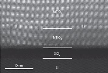
These ferroelectric films are grown on a base of silicon. Alignment of the crystal structures, seen here, is crucial to the efficient transfer of electricity.
As microelectronics get smaller and smaller, one of the biggest challenges to packing a smartphone or tablet with maximum processing power and memory is the amount of heat generated by the tiny “switches” at the heart of the device.
A complex metal oxide film – designed by IBM and University of Texas, Austin (UTA) researchers, and tested at IBM, the National Synchrotron Light Source (NSLS) at Brookhaven National Laboratory, and Oak Ridge National Laboratory (ORNL) – could help reduce the voltage required to switch electronic signals, and thus the excessive energy they require. Their research is published in the October issue of Nature Nanotechnology.
“This project is to develop films that will allow us to decrease the voltage needed to make the switch flip in a nanotransistor,” said Jean Jordan-Sweet, an IBM researcher at NSLS. “The emphasis is on trying to incorporate ferroelectrics into the industry standard silicon-based devices to increase the performance while reducing the need for more voltage.”
A team of researchers, led by IBM researcher Catherine Dubourdieu of the French National Centre for Scientific Research, was able to switch the ferroelectric polarization of these films without the use of a conducting bottom electrode, which could allow for smaller devices that maximize output without excess heat.
To do this, the UTA researchers grew a barium-titanate film on a silicon base using molecular beam epitaxy, a method that deposits a crystalline layer in registry with a single-crystal substrate. Thanks to piezoresponse force microscopy performed at ORNL, the team determined that the resulting material was ferroelectric, meaning it has an electric polarization that can be reversed when an external electric field is applied. This is useful not only for low power logic devices but also for nonvolatile memories.
“These ferroelectric films can switch, and once they’re switched they are stable at room temperature; moreover you can make these things on a really small nanoscale and there are a lot of ways you can incorporate them into microelectronics devices,” Jordan-Sweet said.
Growing the film atop silicon takes finesse. The crystalline structures of barium-titanate and silicon don’t exactly line up, so it’s a bit like trying to get tennis balls to fit into an egg carton. They’re too large for the depressions, so a buffer layer has to be added to ensure that good registry will be made between the two substances. In this case, strontium-titanate was used because its crystal unit size is between that of silicon and barium-titanate, which allows for a gradual re-alignment of the crystal structure in the film.
Once the films were successfully grown, Dubourdieu and Jordan-Sweet used the X20A beamline at NSLS to perform x-ray diffraction tests to characterize the tetragonality – or the “out-of-squareness” of the crystal structure – within the film. They found that the buffer layer induced the correct structure in the barium titanate so that the tetragonal crystal units, and thus the electrical polarization, pointed in the correct direction for making good transistors.
Using piezoresponse force microscopy at Oak Ridge National Laboratory, the team found that they could produce ferroelectric switching within films from 8 to 40 nanometers thick, though a thickness of just 10 nanometers was best to ensure that polarity across the film was evenly distributed.
This work was funded by IBM, the U.S. Department of Energy Office of Science, the National Science Foundation, and the Office of Naval Research.
2013-4331 | INT/EXT | Newsroom


