Technologies Available for License
Category: advanced materials
2013-014: Patterning by Area Selective Oxidation
Invention: 2013-014
Patent Status: U.S. Patent Number 9,221,957 was issued on December 29, 2015
For technical and licensing related questions, email tcp@bnl.gov.
Summary

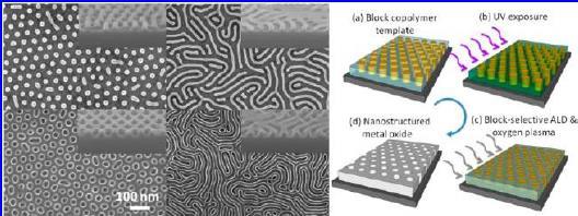
Left: SEM micrographs showing self-assembled PS-b-PMMA thin film templates and corresponding nanostructured Al2O3 patterns created by block-selective deposition. Cylindrical (top left) and lamellar (top right) patterns of initial PS-b-PMMA templates with PMMA removed for the purpose of enhanced SEM contrast. (Bottom) After six TMA/water atomic layer deposition cycles on UV-irradiated (left) cylindrical and (right) lamellar templates with PMMA domains removed prior to the deposition. Insets show the 70° tilted cross-sectional views. Polymers were removed by oxygen plasma etching after deposition. Scale bars in all images denote 100 nm. Right: Schematic description of the modified blockselective metal oxide synthesis. (a) Self-assembled PS-b-PMMA thin film on a Si substrate. A cylindrical phase is given as an example with light blue matrix and yellow cylinders indicating the PS and PMMA domains, respectively. (b) UV irradiation of the polymer template induces preferential chem
Phase-separated block copolymer films have been used to substitute for photoresist in lithography and as nanoscale reactors for controlled synthesis of inorganic materials. Sequential infiltration synthesis (SIS), a method of selectively loading copolymer domains with organometallic precursors and reacting them to form metal oxides, builds on area-selective chemical vapor deposition (CVD) and area-selective atomic layer deposition. The process exposes self-assembled thin films of polystyrene-block-poly(methyl methacrylate) (PS-b-PMMA) to vapors of organometallic precursors selected for their ability to infiltrate the film and bind selectively to the PMMA. It relies on the selective precursor attachment to PMMA during a first growth cycle. Because the SIS process relies on the organometallic precursor binding selectively to the PMMA component of the block copolymer film, not all desired compositions can be grown successfully. The inventors have developed a method of chemically modifying PS-b-PMMA films to enhance their ability to localize weakly interacting species. One example of this is using ultraviolet (UV) irradiation to photo-oxidize the PS domains, with the result that certain precursors now localize to the PS domains rather than to the PMMA domains which are left unaffected by the UV exposure.
Description
Technologies are described for methods for producing a pattern of a precursor on a substrate. The methods may comprise receiving a patterned block copolymer on a substrate. The patterned block copolymer may include a first polymer block domain and a second polymer block domain. The method may comprise exposing the patterned block copolymer to a light effective to oxidize the first polymer block domain in the patterned block copolymer. The method may comprise applying a precursor to the block copolymer. The precursor may infuse into the oxidized first polymer block domain. The method may comprise applying a removal agent to the block copolymer. The removal agent may be effective to remove the first polymer block domain and the second polymer block domain from the substrate, and may not be effective to remove the infused precursor infused into the oxidized first polymer block domain.
Benefits
Chemically modifying PS-b-PMMA films to enhance their ability to localize weakly interacting species broadens the scope of SIS. One example of this is using ultraviolet (UV) irradiation to photo-oxidize the PS domains, with the result that certain precursors now localize to the PS domains rather than to the PMMA domains which are left unaffected by the UV exposure.
Applications and Industries
The nanoscale dimensions offered by this bottom-up technique are useful in semiconductor and optoelectronic devices.
Journal Publication & Intellectual Property
- Chemically Enhancing Block Copolymers for Block-Selective Synthesis of Self-Assembled Metal Oxide Nanostructures (.pdf)
- US 9,221,957 B2 (.pdf)
- Selective sequential infiltration synthesis of ZnO in the liquid crystalline phase of silicon-containing rod-coil block copolymers (.pdf)
Tags: nanostructures
Contacts
-

Poornima Upadhya
Manager Technology Transfer & Commercialization
Technology Commercialization
(631) 344-4711, pupadhya@bnl.gov
-

Avijit Sen
IP Licensing & Commercialization
Technology Commercialization
(631) 344-3752, asen@bnl.gov