Technologies Available for License
Categories: advanced materialsenergy
2014-006: Polycrystalline CuIn(1-x)Ga(x)Se2 (CIGS) based thin-film photovoltaic devices
Invention: 2014-006
Patent Status: U.S. Patent Number 10,333,017 was issued on June 25, 2019
For technical and licensing related questions, email tcp@bnl.gov.
Summary

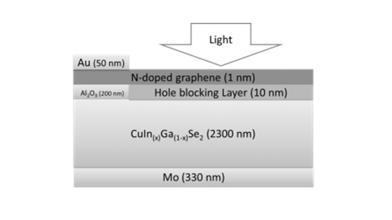
A schematic illustration of an exemplary embodiment of the disclosed CIGS based solar cell, with a quasi-2-dimensional electron extracting layer and an organic hole blocking layer.
Polycrystalline copper indium gallium selenide (CuIn(1-x)Ga(x)Se2 or CIGS) based direct bandgap semiconductors are strong candidates for manufacturing low cost, high-throughput solar energy harvesting thin film photovoltaic devices. State of the art CIGS devices demonstrate 15-18% power conversion efficiencies with best cell performance reaching ca. 20%. However, this is well below the theoretical maximum of 32.8% predicted for the identical material composition with a 1.15 eV. The main reasons for this disparity are due to the effects of parasitic layer absorption and charge recombination at the interface and the bulk of the CIGS layer. This invention describes a novel structure of the CIGS solar cell that affords significantly higher charge transport capability, improved performance, and lower fabrication and maintenance cost by reducing parasitic effects and/or interfacial recombination.
Description
The photovoltaic device of the present invention includes a substrate, a back contact layer, an absorber layer comprising p-doped polycrystalline CuIn(1-x)Ga(x)Se2, where x is between 0.3 and 1, and an n-doped charge-separation/collection layer, said charge-separation/collection layer comprising a graphene or a quasi two-dimensional material. In some examples, the photovoltaic device may further include an organic based hole blocking layer (e.g., phenanthroline) positioned between the absorber layer and the charge-separation/collection layer.
Benefits
Thin film photovoltaic devices require less active material than bulk-type solar cells, reducing raw material cost. With the increase in efficiency offered by this novel structure, CIGS solar cells may offer a lower levelized cost of electricity while being environmentally friendly.
Applications and Industries
This invention is potentially useful in a host of applications, including graphene-semiconductor diodes, batteries, fuel cells, sensors, and solar cells. In addition, a scalable and low-cost doping of graphene could improve technologies in a wide range of fields such as microelectronics, optoelectronics, and energy storage.
Journal Publication & Intellectual Property
- Spontaneous and strong multilayer graphene n-doping on sodalime glass and its application in graphene-semiconductor junctions (.pdf)
- US 10,333,017 B2 (.pdf)
Press Releases
Contacts
-

Poornima Upadhya
Manager Technology Transfer & Commercialization
Technology Commercialization
(631) 344-4711, pupadhya@bnl.gov
-

Avijit Sen
IP Licensing & Commercialization
Technology Commercialization
(631) 344-3752, asen@bnl.gov