Technologies Available for License
Categories: electronics & instrumentationnanotechnology
2015-021: LASER from Ultrathin Disordered Nanoscale Structures
Invention: 2015-021
Patent Status: U.S. Patent Number 10,585,043 was issued on March 10, 2020
For technical and licensing related questions, email tcp@bnl.gov.
Summary

SEM of thin-film coupled nanostructures
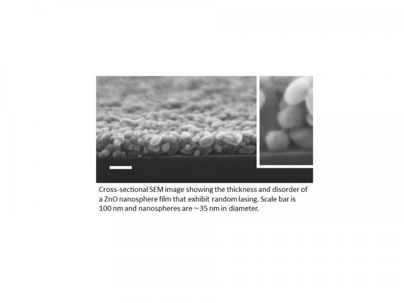
Lasing in solution-processed nanomaterials has gained significant interest because of the potential for low-cost integrated photonic devices. A key challenge is to utilize a comprehensive knowledge of the system's spectral and temporal dynamics to design low-threshold lasing devices. In this invention, intrinsic lasing (without external cavity) at low-threshold in an ultrathin film of coupled, highly crystalline nanospheres with overall thickness on the order of lambda/4 is demonstrated. The cavity-free geometry consists of ~35 nm zinc oxide nanospheres that collectively localize the in-plane emissive light fields while minimizing scattering losses, resulted in excitonic lasing with fluence thresholds at least an order of magnitude lower than previous UV-blue random and quantum-dot lasers (<75 µJ/cm>sup>2).
Description
This invention demonstrates a laser consisting of nanoscale semiconductor structures that are assembled together in a film form that has overall nanoscale dimensions that are smaller than the free space emission wavelength. This differs from other nanoscale lasers where either quantum-confinement or strong resonant scattering is required to generate the nonlinear response. As such, one can avoid the use of thick devices which would otherwise be needed to provide the required gain. The end result is an ultrathin-film device which is at least 10 times thinner and exhibit lasing action with at least an order of magnitude lower in the required energy input. The mechanism that triggers the lasing at low energy input is the increase of light interaction within the nanoscale material due to a better packing density while the decrease in void (separation between the nanoscale structures) reduces the various loss mechanisms. Precisely, this was demonstrated with films that are fabricated with nanoscale structures that have average size of about 35 nm and made of highly crystalline zinc oxide. Originally dispersed in a solvent (e.g., ethanol), the nanoscale structures were spin-coated on a substrate. Subsequently, the solvent was evaporated via thermal methods. While spin-coating was initially used to create the film, other techniques such as nanoimprint lithography, dip coating, inkjet printing and matrix-assisted pulse laser evaporation can be used to create similar films. Furthermore, other highly crystalline nanoscale structures can be used as the lasing material. This extends to material systems such as nitrides and oxides (II-VI and III-V semiconductors), where they intrinsically possess gain (the ability to create lasing) can be nanostructured and assembled in a film form to now create lasing. Alternatively, lasing dyes typically used in solution can be deposited or mix with such nanoscale structures (10-100 nm) to create lasing in this newly demonstrated size regime.
Benefits
This invention suggests that coupled, highly crystalline nanostructures, fabricated by low cost solution processing methods, can function as viable building blocks for high-performance optoelectronic devices.
Applications and Industries
The applications for this technology include developing highly stable monochromatic light source, hand-held or miniaturized devices for imaging and sensing, and optoelectronic devices that require light-emitting elements.
Journal Publication & Intellectual Property
- Excitonic Lasing in Solution-Processed Subwavelength Nanosphere Assemblies (.pdf)
- US 10,585,043 B2 (.pdf)
Tags: optoelectronic
Contacts
-

Poornima Upadhya
Manager Technology Transfer & Commercialization
Technology Commercialization
(631) 344-4711, pupadhya@bnl.gov
-

Avijit Sen
IP Licensing & Commercialization
Technology Commercialization
(631) 344-3752, asen@bnl.gov