Technologies Available for License
Category: electronics & instrumentation
2022-005: A User-Configurable High-Speed Line Driver
Invention: 2022-005
Patent Status: U.S. Patent Number 122,065,302 was issued on January 21, 2025
For technical and licensing related questions, email tcp@bnl.gov.
Summary

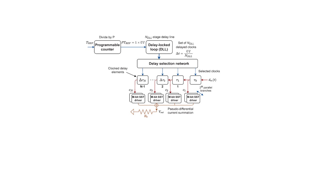
Top-level block diagram of the adaptive line driver circuit.
Existing transmitter designs for integrated high-speed wired links (known as line drivers) are application specific. As a result, they require system-wide redesign by a designer before they can be used for links with different cable parameters and/or data rates. Brookhaven researchers provided an improved high-speed line-driver circuit that uses a built-in delay-locked loop (DLL) to allow the duration of each pre-emphasis interval to be adaptively programmed. As a result, a much wider range of output waveforms with pre symbol or post-symbol boosting can be generated. In turn, such flexibility would allow for the users to optimize the driver parameters on-the-fly to handle a variety of application scenarios and/or in the presence of process, voltage, and temperature (PVT) variations.
Description
The adaptive line driver circuit includes a delay-locked loop (DLL) circuit, which includes a phase detector (PD) circuit, charge pump (CP) circuit, and voltage-controlled delay line (VCDL) circuit operatively coupled together. The delay-locked loop circuit provides user-configurable durations of pre-emphasis and feed-forward equalization of the signal. The delay locked loop circuit also provides a user-configurable parameter including at least one of pre-data tap amplitude, data tap amplitude, post-data tap amplitude, pre-data tap duration, post-data tap duration, pre-data tap quantity, and post-data tap quantity. The adaptive line driver circuit further includes an array of source-series terminated (SST) driver circuits operatively coupled to the delay-locked loop circuit and used to drive respective data taps. These arrays can also be programmed by the user to configure nominal and pre-emphasized data swing.
Benefits
The proposed circuit offers a fully integrated CMOS line driver circuit that includes a variety of user configurable settings, thus allows for users to find optimal driver settings based on their specific line and load. These user settings will have both coarse and fine variability, thus allows for the driver to fit a variety of applications and also adjust slightly to account for process-voltage-temperature (PVT) variations.
Applications and Industries
The driver is a low-power variable impedance source-series terminated (SST) driver for high-loss cabling or any other applications where impedance matching is less critical.
Journal Publication & Intellectual Property
- US 12,206,530 B2 (.pdf)
- A low-power 1 Gb/s line driver with configurable pre-emphasis for lossy transmission lines (.pdf)
- Self-Adaptation of Line Driver Pre-Emphasis Parameters via Embedded Line Loss Sensing (.pdf)
- Testing of a Line Driver With Configurable Pre-Emphasis on Lossy Transmission Lines (.pdf)
Tags: ASIC
Contacts
-

Poornima Upadhya
Manager Technology Transfer & Commercialization
Technology Commercialization
(631) 344-4711, pupadhya@bnl.gov
-

Avijit Sen
IP Licensing & Commercialization
Technology Commercialization
(631) 344-3752, asen@bnl.gov