Technologies Available for License
Category: electronics & instrumentation
2022-018: Charge-sensitive amplifier for use in radiation detection and spectroscopy
Invention: 2022-018
Patent Status: Application Number WO 2024/086081 A1 was published on April 25, 2025
For technical and licensing related questions, email tcp@bnl.gov.
Summary

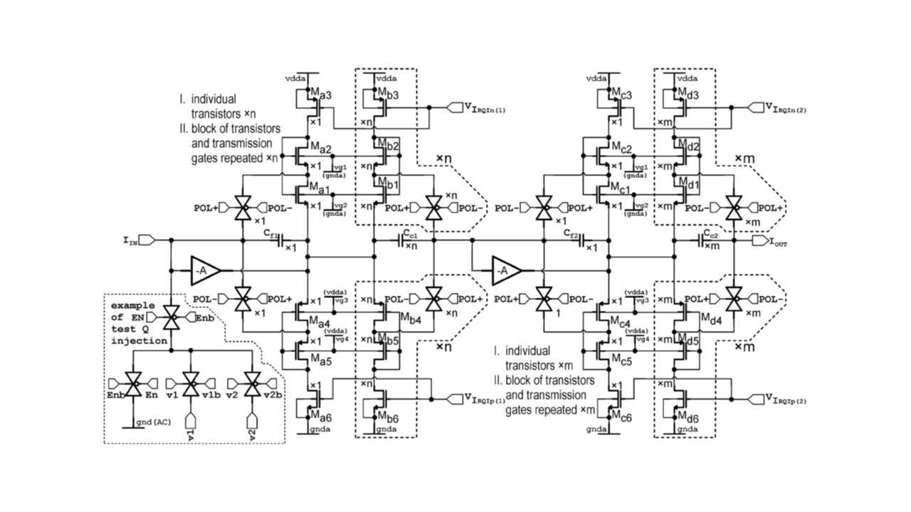
Figure: Illustration of a two-stage cascaded CSA using the SCFET circuit network in charge integration and pole-zero cancellation of both stages and is preceded by switches in both stages, which is suitable for compensating I(leak) that flows into the I(IN) port, is operationally configured using the pole-zero cancellation architecture, is operable with either holes or electrons depending on which switches are programmed or dynamically switched on, and yields multiplication of the input charge signal by the gain factor nxm.
The CSA can be used for readout ASICs for x-ray sensors, in particular fine pitch pixel detectors (small footprint pixels) without a stabilizing capacitor and still able to operate stably regardless of the levels of sensor leakage current and coping with high rates of incoming X-ray events; and it can be single stage built with a self-cascoded feedback circuit or more stages can be cascaded before direct coupling to a shaping filter and, after the shaping filter, to a discriminator providing also a leakage current compensation alternative that can be used alone or can be configured into a pole-zero cancellation system that is an improvement over the previous feedback circuit (Krummenacher feedback circuit) and p-z cancellation systems respectively.
Description
The charge-sensitive amplifier is developed by utilizing a self-cascoded-field effect transistor (SCFET) circuit network or a self-cascoded bipolar-junction transistor (SCBJT) circuit network connected in a feedback path of a high-open loop-gain amplifier. In this connection, three terminals are distinguished from the use of only two terminals of such a self-cascoded circuit network. This is done to ensure, on the one hand, that this circuit network is connected in a feedback loop with a minimum voltage difference between the input of the feedback loop and its output, and on the other hand, to ensure that the bias current is sufficient for active operation of the circuit network. The CSA can be configured with the feedback network as an integrator only, thereby converting the charge liberated in the ionization process into a step voltage that decays back to the baseline with a speed depending on an effective time constant of the circuit network (i.e., by forming a leaky integrator). Alternatively, by incorporating one or more replicas of the feedback network electrically connected in parallel, the CSA can be configured in a system with pole-zero cancellation, the output of which is a charge packet equal to the input charge packet multiplied by a gain factor. The resulting charge signal can further be processed in filters or passed through consecutive stages of filtering and amplification. Therefore, two or more stages can be cascaded to achieve high charge multiplication I(OUT)=m×n×I(IN).
Benefits
Unlike conventional techniques, which include common gate feedback, the CSA does not require a reference voltage to control active devices in the feedback path of the CSA. This feature advantageously avoids undesirable crosstalk between a source of the reference voltage and amplified voltage signals.
Applications and Industries
This CSA can be used in various applications including radiation detection and energy spectroscopy.
Journal Publication & Intellectual Property
Contacts
-

Poornima Upadhya
Manager Technology Transfer & Commercialization
Technology Commercialization
(631) 344-4711, pupadhya@bnl.gov
-
Avijit Sen
IP Licensing & Commercialization
Technology Commercialization
(631) 344-3752, asen@bnl.gov