Pressing Out Clean Interfaces in Layered 2D Devices
May 31, 2022
 enlarge
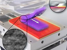
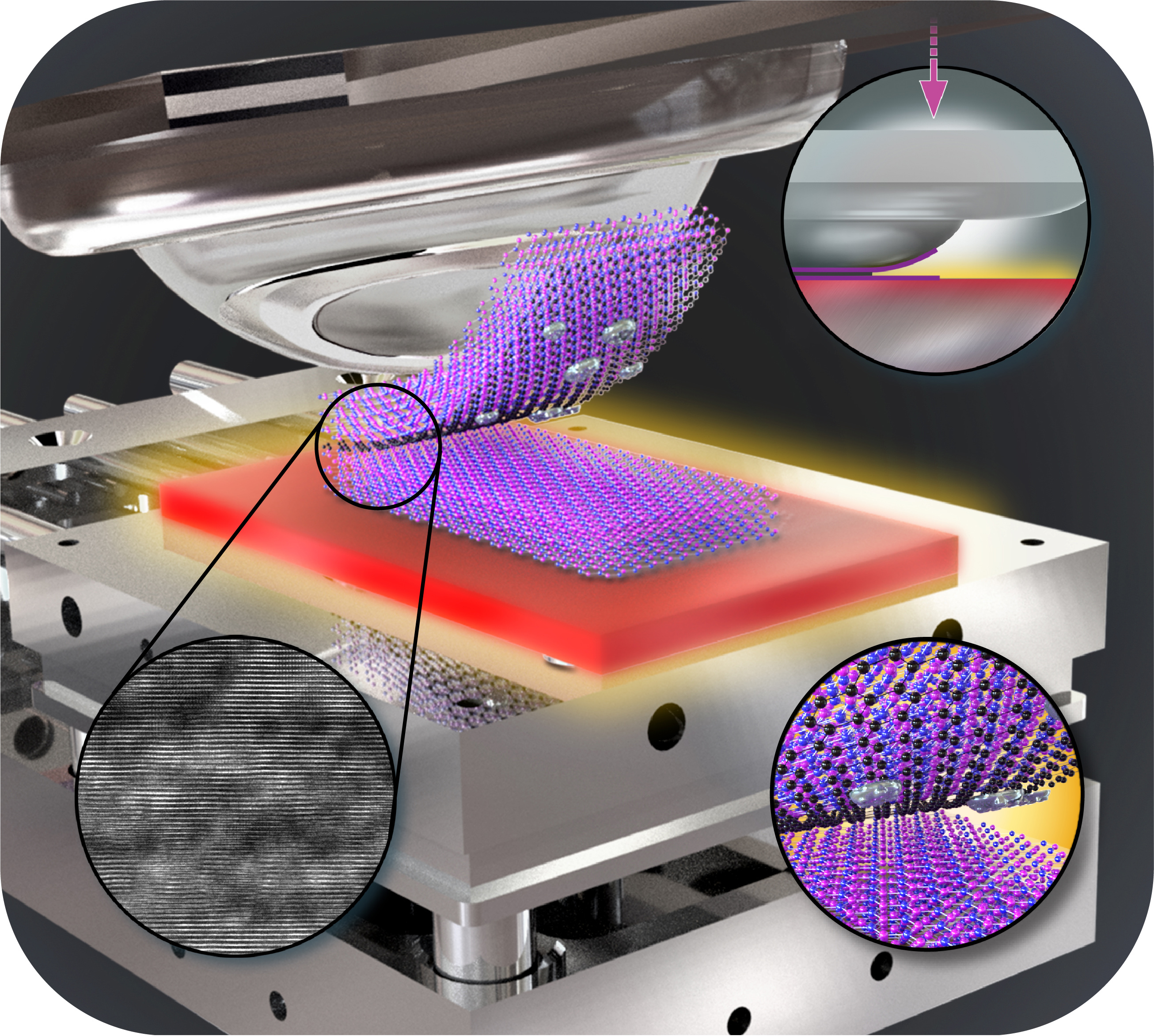
Stacking 2D layers on a heated substrate and applying pressure pushes out residues from contaminated graphene to form clean interfaces (TEM image, bottom inset).
What is the Scientific Achievement?
CFN collaborators and staff demonstrated systematic fabrication of atomically clean graphene heterostructures with record large dimensions (as large as 7,500 µm2 ). The team illuminated a new cleaning mechanism, combining mechanical actuation and thermal activation, that achieves atomically-clean 2D layers for use in state-of-the-art devices.
What is the Significance and Impact?
This cleaning mechanism is an important tool for developing manufacturing protocols for large and high-quality devices and obviates additional post-cleaning processes.
Research Details
- This work was made possible by the unique process control provided by CFN Quantum Material Press (QPress).
- DFT calculations describe the interactions between the polymer residues and the 2D layers.
- The CFN Electron Microscopy, Materials Synthesis, and Theory & Computation Facilities were used in this study.
This study showed that the interface cleaning process of layered heterostructures made from polymer-contaminated 2D layers involves more complex mechanisms than a simple thermal actuation that has been used to make clean interfaces. The combination of non-bonding interactions of polymer with graphene, thermally activated mobilization of polymer residues, and mechanical actuation is essential for fabricating heterostructures with atomically clean interfaces. This approach allowed us to fabricate record large-area clean device out of PVA-contaminated graphene. This study opened a new opportunity to develop more effective manufacturing process to make large and clean layered heterostructure devices.
This study used multiple resources of CFN. The systematic experiments on the effects of thermal activation and mechanical actuation on the cleaning process was conducted using a “Stacker”, i.e., a motorized 2D material transfer module, of QPress cluster tool (a new user facility at CFN for 2D material fabrication/characterization). Density functional theory (DFT) calculations was done to understand the interactions between the polymer residues (i.e., PVA) and 2D layers (i.e., graphene). The interfaces of the heterostructure were examined by cross-sectional HRTEM imaging and EDS analysis.
Publication Reference
Z. Huang, E. Cuniberto, S. Park, K. Kisslinger, Q. Wu, T. Taniguchi, K. Watanabe, K. G. Yager, D. Shahrjerdi, “Mechanisms of Interface Cleaning in Heterostructures Made from Polymer-Contaminated Graphene.” Small 18, 20 (2022).
DOI: 10.1002/smll.202201248
https://onlinelibrary.wiley.com/doi/10.1002/smll.202201248
Acknowledgment of Support
The authors acknowledge partial financial support from NSF (grants EECS- 1940764). K.W. and T.T. acknowledge support from the Elemental Strategy Initiative conducted by the MEXT, Japan (Grant Number JPMXP0112101001) and JSPS KAKENHI (Grant Numbers 19H05790, 20H00354 and 21H05233). This work was performed in part at the ASRC Nano Fabrication Facility of CUNY in New York. This research used resources of the Center for Functional Nanomaterials (CFN), which is a U.S. Department of Energy Office of Science User Facility, at Brookhaven National Laboratory under Contract No. DE-SC0012704. D.S. acknowledges Prof. J. Uichanco at the University of Michigan Ann Arbor and Dr. C. Black at the Center for Functional Nanomaterials at BNL for helpful discussions.
2022-20809 | INT/EXT | Newsroom