Research Highlight: How Heat Heals Graphene Nanoribbons
May 13, 2015
What Is The Scientific Achievement?
 enlarge
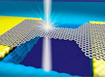
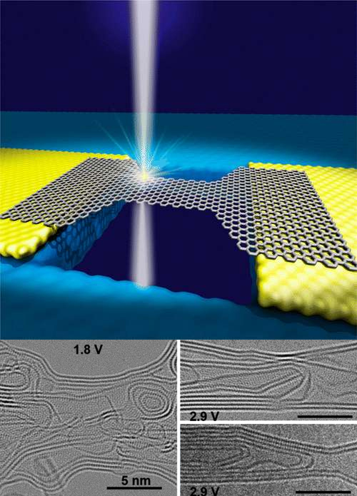
Top: Schematic of a suspended graphene ribbon, being imaged in the transmission electron microscope. Bottom: atomic resolution electron microscopy images of graphene ribbons (left: 1.8 V) at low applied voltage/temperature and (right: 2.9 V) following high voltage/temperature heating. The ribbons possess fewer defects and exhibit improved alignment in the direction of current flow after heating.
The use of graphene and other two-dimensional materials in next-generation electronics is hampered by the significant damage caused by conventional lithographic processing techniques employed in device fabrication. To reduce the density of defects and increase mobility, direct resistance heating (Joule heating) is often used since it facilitates lattice reconstruction and promotes self-repair. Despite its importance, an atomistic understanding of the structural and electronic enhancements in graphene devices fashioned in this way is still lacking. This work used a combination of experimental and theoretical methods from CFN’s Electron Microscopy and Theory & Computation Facilities, respectively, to understand how this process occurs. Graphene nanoribbon devices were fabricated and electrically measured in situ to the sample chamber of an aberration-corrected transmission electron microscope. The observations showed directly how the structures initially had highly irregular sp2-bonded edges, and monitored how the application of increasing levels of Joule heat led to a transformation of the structure towards sharp, faceted edges.
Computational simulations showed that this is a result of concentrated local currents at lattice defects, which in turn promotes restructuring of unfavorable edge structures toward an atomically sharp state. Measurements of the conductivity of the devices established that the process doubles the inherent electrical performance of the graphene nanoribbons, and that this is associated with a 3-fold reduction in ribbon width due to the improved crystallinity. These observations demonstrate how how electronic structure can be tailored through specific graphene nanoribbon configurations and controlled sample annealing.
Why Does This Matter?
For graphene to fulfill its promise as the conducting component in future integrated circuit technologies, robust device fabrication approaches must be developed for it. This study clarified the atomic-scale mechanism by which the most popular approach—electrically driven heating—shapes the structure of graphene and improves its overall performance.
What Are The Details?
- CFN Capabilities: CFN’s Electron Microscopy Facility’s aberration-corrected transmission electron microscope was used for its atomic resolution imaging capabilities and its ability for electrically driven sample heating.
Publication Reference
Electronic Transport of Recrystallized Freestanding Graphene Nanoribbons
Zhengqing John Qi,1 Colin Daniels,2 Sung Ju Hong,1,2 Yung Woo Park,3 Vincent Meunier,2 Marija Drndić,1 and A. T. Charlie Johnson1
1 Department of Physics and Astronomy, University of Pennsylvania, Philadelphia, Pennsylvania 19104, United States,
2 Department of Physics, Applied Physics, and Astronomy, Rensselaer Polytechnic Institute, Troy, New York 12180, United States
3 Department of Physics and Astronomy, Seoul National University, 1 Gwanak-ro, Gwanak-gu, Seoul, 151-747, Korea
Nano Letters 9, 3510 (2015)
Acknowledgment of Support
This work was supported by SRC Contract # 2011-IN-2229, which is associated with the NSF AIR Program ENG-1312202. Z.J.Q. acknowledges support from the IBM Ph.D. Fellowship and the NSF IGERT program (Grant DGE02-21664). C.D. and V.M. acknowledge support from New York State under NYSTAR Contract C080117. All calculations were performed at the Center for Computational Innovation at Rensselaer Polytechnic Institute. Y.W.P. and S.J.H. acknowledge support from the Leading Foreign Research Institute Recruitment Program (0409-20100156) of NRF and the FPRD of BK21 through the MEST, Korea. M.D. acknowledges funding from the NIH Grant R21HG006313 and the Nano/Bio Interface Center through the National Science Foundation NSEC DMR08-32802. Research was carried out in part at the Center for Functional Nanomaterials, Brookhaven National Laboratory, which is supported by the U.S. Department of Energy, Office of Basic Energy Sciences, under Contract No. DE-AC02-98CH10886. We acknowledge support for access of the FEI-Titan ACTEM through proposal 31972 at Brookhaven National Laboratory's Center for Functional Nanomaterials. The authors thank Dr. Julio A. Rodrigues-Manzo for TEM imaging, analysis, and discussions.
2015-5707 | INT/EXT | Newsroom