Writing at the Nanoscale
Brookhaven's "Electro Pen" may impact a host of developing nanotechnologies
August 28, 2005
UPDATE: The Electro Pen Nanolithography technique is now described in a research article published in the October 29, 2005, online edition of the Journal of the American Chemical Society. The article details more fully the advantages of EPN, particularly its unique ability to deposit layers of "ink" with an integer number of molecular layers ranging from a single layer to several layers.
UPTON, NY — At the U.S. Department of Energy's Brookhaven National Laboratory, scientists have developed a new chemical "writing" technique that can create lines of "ink" only a few tens of nanometers, or billionths of a meter, in width.
"Our new 'writing' method opens up many new possibilities for creating nanoscale patterns and features on surfaces. This may have a significant impact on developing nanotechnologies that involve nanopatterning, such as molecular electronics — tiny circuits built using single organic molecules," said Brookhaven Lab physicist Yuguang Cai. Cai will discuss the method at the 230th American Chemical Society national meeting in Washington, D.C., on Sunday, August 28, at 12 p.m. in room 8-9 of the Renaissance Hotel.
Cai and his colleagues call the technique "Electro Pen Nanolithography" (EPN). They sweep a very thin metal tip across a film of organic molecules. The tip carries an electric voltage, which causes the region under it to "oxidize," or undergo a reaction that changes the chemical makeup of the film. In a single sweep of the pen, organic "ink" molecules are transferred from the tip to the oxidized regions, creating an extremely thin line.
 enlarge
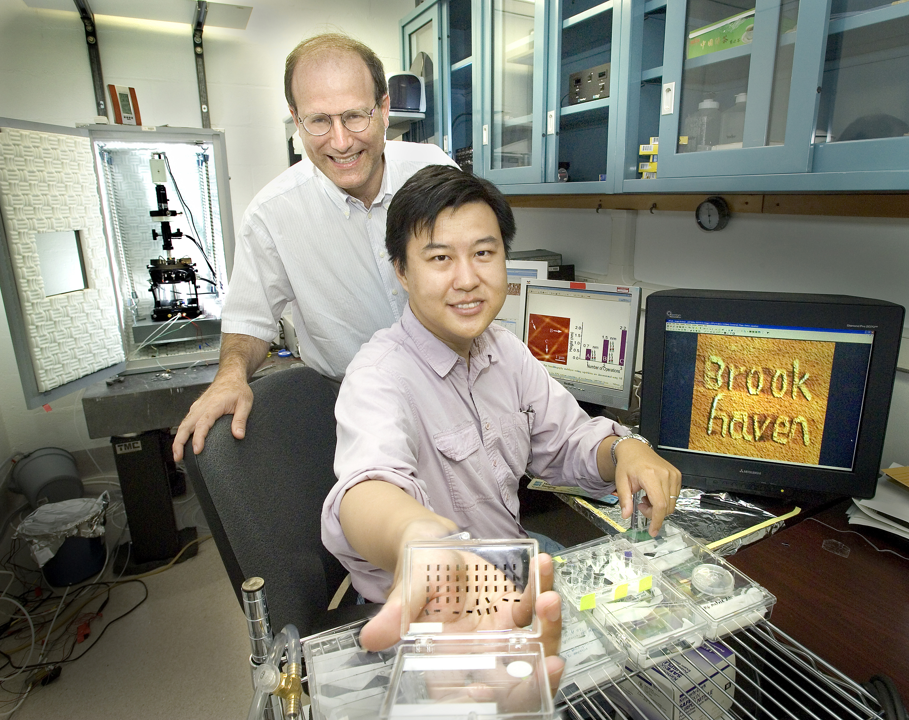
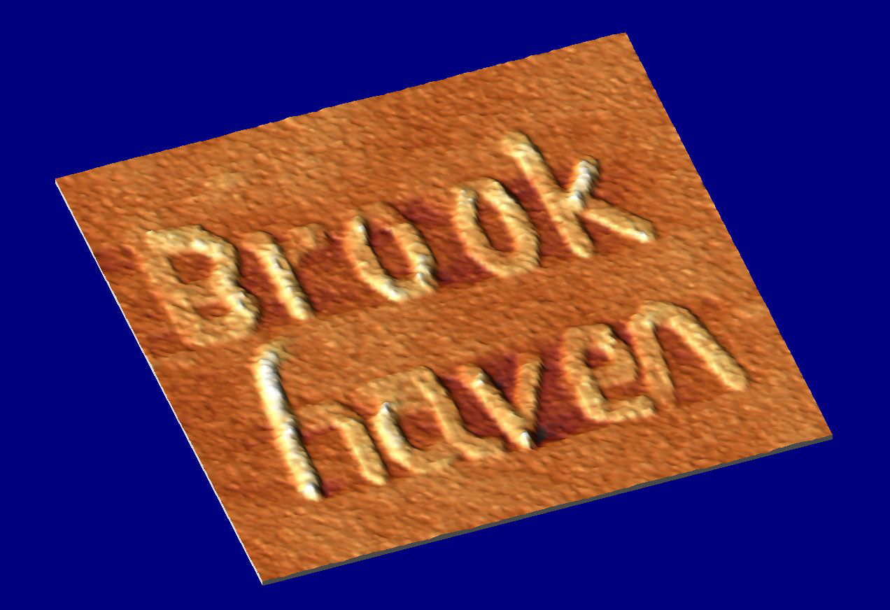
"Written" with the Electro Pen, the lines forming these words are 150 nanometers wide and less than one nanometer high. They are made of organic molecules. (Click image to download hi-res version.)
Each line is just one molecule thick, but the researchers can produce multilayered patterns by writing over the existing pattern. This gives them the ability to create three-dimensional nanoscale "landscapes." Moreover, by turning off the voltage, they can use the tip as a tiny "scanner" to "read" and create an image of the pattern just written.
With further research, EPN may have the ability to "write" biomolecular materials, such as proteins, onto surfaces. These nanoscale protein deposits might, for example, serve as biosensors.
This research is supported by the Office of Basic Energy Sciences within the U.S. Department of Energy's Office of Science.
2005-10359 | INT/EXT | Newsroom