Atomically Thin Magnets for Next Generation Spin and Quantum Electronics
Stevens researchers develop a ferromagnetic semiconductor that works at room temperature, solving one of science's most intractable problems
June 30, 2020
 enlarge
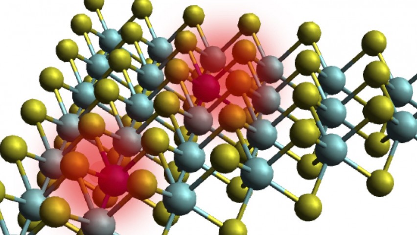
A two-atom-thick ferromagnetic semiconductor. The green, blue, and red spheres are sulfur, molybdenum, and iron atoms, respectively. Credit: Stevens Institute of Technology.
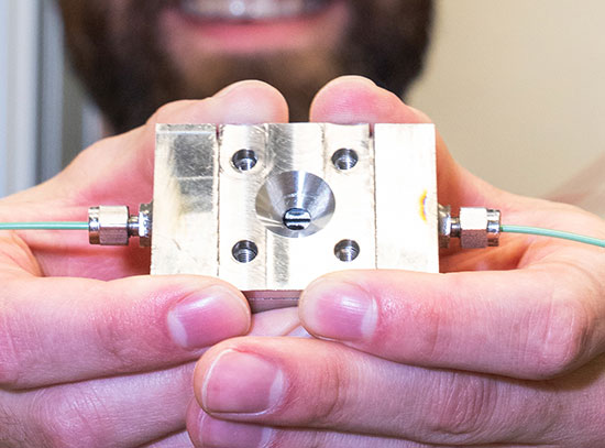
This news release, published by Stevens Institute of Technology, describes a study recently featured in Nature Communications on an atomically thin magnetic semiconductor. As the collaborative team reported, iron atoms take the place of some molybdenum atoms in single layers of molybdenum disulfide to give rise to room-temperature ferromagnetism, which could be leveraged for next-generation electronics. This research was in part conducted in the Electron Microscopy Facility of the Center for Functional Nanomaterials (CFN)—a U.S. Department of Energy (DOE) Office of Science User Facility at Brookhaven National Laboratory. Here, under a CFN user proposal, Stevens mechanical engineering professor EH Yang led the work to perform critical imaging and spectroscopy experiments with CFN staff scientist Lihua Zhang. The other collaborating institutions are Columbia University, Rensselaer Polytechnic Institute, and University of Rochester.
(Hoboken, N.J – May 13, 2020) – As our smartphones, laptops, and computers get smaller and faster, so do the transistors inside them that control the flow of electricity and store information. But traditional transistors can only shrink so much. Now, researchers at Stevens Institute of Technology have developed a new atomically thin magnetic semiconductor that will allow the development of new transistors that work in a completely different way; they not only can harness an electron’s charge but also the power of its spin, providing an alternative path to creating ever smaller and faster electronics.
Rather than relying on making smaller and smaller electrical components, the new discovery, reported in the April 2020 issue of Nature Communications, potentially provides a critical platform for advancing the field of spintronics (spin + electronics), a fundamentally new way to operate electronics and a much-needed alternative to continued miniaturization of standard electronic devices. In addition to removing the miniaturization barrier, the new atomically thin magnet can also enable faster processing speed, less energy consumption and increased storage capacity.
“A two-dimensional ferromagnetic semiconductor is a material in which ferromagnetism and semiconducting properties coexist in one, and since our material works at room temperature, it allows us to readily integrate it with the well-established semiconductor technology,” said EH Yang, a professor of mechanical engineering at Stevens Institute of Technology, who led this project.
“The magnetic field strength in this material is 0.5 mT; while such weak magnetic field strength cannot allow us to pick up a paper clip, it is large enough to alter the spin of electrons, which can be utilized for quantum bits applications,” said Stefan Strauf, a professor of physics at Stevens.
When computers were first built, they filled an entire room, but now they can fit in your back pocket. The reason for this is Moore’s law, which suggests that every two years, the number of transistors that fit on a computer chip will double, effectively doubling a gadget's speed and capability. But transistors can only become so small before the electrical signals that they are supposed to control no longer obey their commands.
While most forecasters expect Moore's law will end by 2025, alternative approaches, which do not rely on physical scaling, have been investigated. Manipulating the spin of electrons, instead of relying solely on their charge, may provide a solution in the future.
Building a new magnetic semiconductor using two-dimensional materials – that is, two-atoms thick– will allow the development of a transistor to control electricity with control of the spin of an electron, either up or down, while the whole device remains lightweight, flexible and transparent.
Using a method called in situ substitutional doping, Yang and his team successfully synthesized a magnetic semiconductor whereby a molybdenum disulfide crystal is substitutionally doped with isolated iron atoms. During this process, the iron atoms kick off some of the molybdenum atoms and take their place, in the exact spot, creating a transparent and flexible magnetic material – again, only two-atoms thick. The material is found to remain magnetized at room temperature, and since it is a semiconductor, it can directly be integrated into the existing architecture of electronic devices in the future.
Yang and his team at Stevens worked with several institutions to image the material – atom by atom – to prove that the iron atoms took the place of some of the molybdenum atoms. These institutions included the University of Rochester, Rensselaer Polytechnic Institute, Brookhaven National Laboratory, and Columbia University.
“To do something great in science, you need to get others to collaborate with you,” said Shichen Fu, a Ph.D. student in mechanical engineering at Stevens. “This time, we brought all the right people together – labs with different strengths and different perspectives – to make this happen.”
— Stevens —
About Stevens Institute of Technology
Stevens Institute of Technology is a premier, private research university situated in Hoboken, New Jersey. Since our founding in 1870, technological innovation has been the hallmark of Stevens’ education and research. Within the university’s three schools and one college, 7,300 undergraduate and graduate students collaborate closely with faculty in an interdisciplinary, student-centric, entrepreneurial environment. Academic and research programs spanning business, computing, engineering, the arts and other disciplines actively advance the frontiers of science and leverage technology to confront our most pressing global challenges. As Stevens celebrates its 150th anniversary, the university continues to be consistently ranked among the nation’s leaders in career services, post-graduation salaries of alumni, and return on tuition investment.
Stevens media contact: Thania Benios, 917-930-5988, thania.benios@stevens.edu
2020-17237 | INT/EXT | Newsroom