Photonic Waveguides Suppress "Crosstalk among Neighbors"
July 22, 2015
What Is The Scientific Achievement?
 enlarge
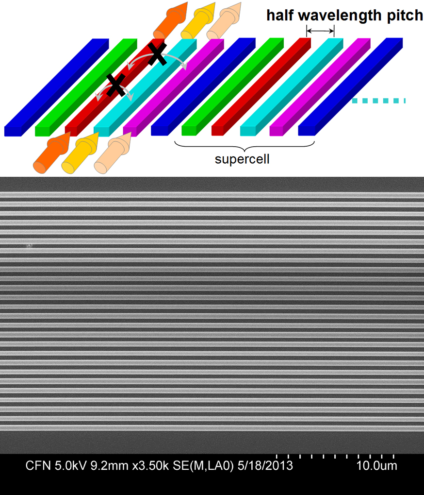
High-density silicon waveguides (26 shown) that have a half-wavelength pitch (a=780nm for λ=1550nm) and fill 50% of the surface area of the underlying substrate have been engineered to achieve inter-waveguide crosstalk below -20dB, paving the way for high-density integrated optical chips.
Silicon photonics holds great promise for low-cost, large-scale integration of photonic components. The demand for increasing density of these components has led to a multitude of technological challenges in their manufacture and operation. Waveguides are perhaps the most ubiquitous component in silicon photonics. One major obstacle is the amount of crosstalk between adjacent optical waveguides, which is the sum of light in one waveguide coupled from neighboring waveguides. Crosstalk can become profound when the distance between adjacent waveguides is smaller than the wavelength (λ) of the light propagating through them. To address this issue, advanced waveguide superlattices were designed and fabricated, comprising an array of waveguides spaced at a pitch of 0.78 μm (λ/2). Such waveguide superlattices can potentially lead to significant reduction in on-chip estate for waveguide elements and salient enhancement of performance for important applications, opening up possibilities for half-wavelength-pitch optical phased arrays and ultra-dense space-division multiplexing. The detected crosstalk was no larger than -20 dB, a level that confirmed the feasibility of these superlattices in photonic device applications.
Why Does This Matter?
This is the first report of the high density integration of silicon waveguides with a half-wavelength pitch. Furhter, low crosstalk was observed for several critical optical communications wavelength bands, such as the 1.505–1.570 μm range, which affords significant opportunities for enhanced optical systems, such as spectrometers and optical-phased arrays.
What Are The Details?
CFN Capabilities: CFN’s Nanofabrication Facilities were used for nano-fabrication and electron microscopy.
Publication Reference
High-Density Waveguide Superlattices with Low Crosstalk
Weiwei Song1, Robert Gatdula1, Siamak Abbaslou1, Ming Lu2, Aaron Stein2, Warren Y.-C. Lai1,3, J. Provine4, R. Fabian W. Pease4, Demetrios N. Christodoulides5, and Wei Jiang1,3,6
1Department of Electrical and Computer Engineering, Rutgers University, Piscataway, NJ 08854, USA
2Center for Functional Nanomaterials, Brookhaven National Laboratory, Upton, NY 11973, USA
3Institute for Advanced Materials, Devices, and Nanotechnology, Rutgers University, Piscataway, NJ 08854, USA
4Department of Electrical Engineering, Stanford University, Stanford, CA 94305, USA
5School of Optics/CREOL, University of Central Florida, Orlando, Florida 32816-2700, USA
6College of Engineering and Applied Sciences and National Laboratory of Solid State Microstructures, Nanjing University, Nanjing 210093, P. R. China
Nature Communications 6, 7027 (2015).
Acknowledgement of Support:
This research was carried out in part at the Center for Functional Nanomaterials, Brookhaven National Laboratory, which is supported by the U.S. Department of Energy, Office of Basic Energy Sciences, under Contract No. DE-AC02-98CH10886. This work is supported in part by U.S. Air Force Office of Scientific Research under Grant No. FA9550-08-1-0394 and by the DARPA Young Faculty Award under Grant No. N66001-12-1-4246.
2015-5849 | INT/EXT | Newsroom