Technologies Available for License
Categories: advanced materialselectronics & instrumentation
2011-008: Reactive Ion Etching of Monolayer and Multilayer Materials
Invention: 2011-008
Patent Status: U.S. Patent Number 9,153,453 was issued on October 6, 2015
For technical and licensing related questions, email tcp@bnl.gov.
Summary

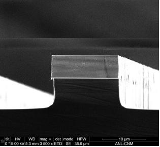
SEM cross-section micrograph of etched multilayers
The invention describes two novel etching process that can be used to etch monolayer and multilayer structures made from a variety of materials such as tungsten and tungsten silicides. The etched materials can be potentially used in a wide range of fields such as semiconductor fabrication, MEMS (microelectromechanical systems), and refractive X-ray optics.
Description
This invention describes mainly two reactive ion etching processes for sectioning by etching of monolayer and multilayer materials. The etching processes use a combination of fluorine, oxygen and other halogen gases. The main differences are about the gases, temperature or the number of steps involved into the etching processes. The silicide-based or organo-metallic monolayers that can be etched are WSi2, VSi2, MoSi2, Si, Mo, Ni, Al2O3, or W. The silicide-based or organo-metallic multilayer that can be etched include WSi2/Si, W/Si, W/B4C, W/C, Mo/Si, MoSi2/Si, Mo/B4C, Ni/B4C, Al2O3/B4C, VSi2/Si.
Benefits
Unlike other currently used etching processes this invention describes single step processes that does not require any intervening passivation step. The processes provide for high anisotropy, adequate sidewall roughness control and high etching rates of both monolayer and multilayer structures made from a variety of materials. In addition, the processes can be carried out at room temperature.
Applications and Industries
The processes are useful for thin multilayer reflective geometry for soft X-ray grading and etching thin monolayers to produce zone plates. The processes are also useful for semi-conductor applications. In addition, the processes can be utilized for the fabrication of multilayer materials, such as a multilayer laue lens, waveguides, hard X-ray zone plates and gratings.
Journal Publication & Intellectual Property
- US 9,153,453 B2 (.pdf)
- WSi2/Si Multilayer Sectioning by Reactive Ion Etching for Multilayer Laue Lens Fabrication (.pdf)
- Advanced multilayer Laue lens fabrication at NSLS-II (.pdf)
Tags: optics
Contacts
-

Poornima Upadhya
Manager Technology Transfer & Commercialization
Technology Commercialization
(631) 344-4711, pupadhya@bnl.gov
-

Avijit Sen
IP Licensing & Commercialization
Technology Commercialization
(631) 344-3752, asen@bnl.gov