25th Anniversary of Rehak's and Gatti's Innovative Detector
December 19, 2008
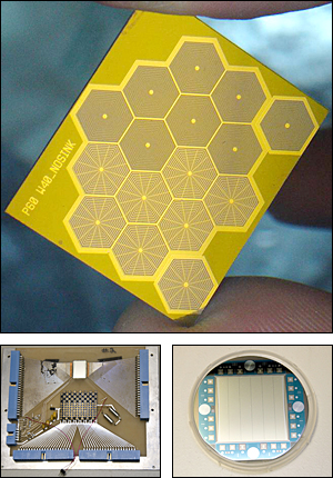
Silicon drift detectors, past to present, 25 years old (bottom, left), 10 years old (bottom, right), and current (top)
Brookhaven's Instrumentation Division develops state-of-the-art instrumentation required for experimental research programs at BNL and throughout the world. Much of their work is focused on detectors that track particles after a collision or detectors that identify the energy and location of absorbed x-rays. Some of the current silicon detector developments are for RHIC and ATLAS upgrades, NSLS and NSLS-II, and NASA missions, to name a few.
These cutting-edge detectors illustrate the extreme versatility of silicon as an ionization sensing medium. A particularly transformative example of this versatility is reflected in the invention of two creative scientists, Pavel Rehak of BNL and Emilio Gatti of the Polytechnic Institute of Milan. In 1983, they published a paper on their invention of the silicon drift detector (SDD), followed later by a patent on this new concept.
The SDD and two other devices outlined in the paper introduced the concept of lateral collection of electric charges with respect to its electrodes, a radical change from the usual longitudinal collection. These new devices therefore permitted charge collection from a large area onto a small-sized anode, resulting in high spatial and ionization-charge accuracy over much larger areas than previously possible with a single detector.
Applications, Developments

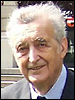
How did two physicists, Pavel Rehak (left) and Emilio Gatti, co-invent the same device a continent apart? More...
Once the SDD was in production, it was first used at CERN, the European particle physics accelerator in Switzerland, in the CERES and WA98 experiments and then at BNL's Relativistic Heavy Ion Collider in the STAR experiment, which used nearly 300 SDDs.
Continued development of the SDD has resulted in further advances in its performance, together with applications that range from mapping the surfaces of celestial bodies in space to detecting forged reproductions of artwork.
One example: Instrumentation, in collaboration with the NASA Marshall Space Flight Center, developed silicon drift detectors for x-ray spectroscopy, which use an array of hexagonal-shaped detectors. These SDDs are shielded from visible light by the use of a thin aluminum layer but are sensitive to soft x-rays. These x-ray detectors are the first in a generation of sensors that may be used on future space missions, in order to map surfaces of various solar bodies with x-ray fluorescence, including the moon (which reflects solar x-rays), Mercury, asteroids, Martian satellites, and Europa, Jupiter's moon.
Silicon wafers undergoing inspection and testing
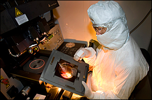
The silicon detectors are fabricated in the clean room of the Instrumentation Division's silicon-detector processing facility, overseen by Zheng Li. By building an electrode structure on both sides of a silicon wafer, a uniform electric field is established with a collecting anode at the center or edge of the detector area.
When a charged particle traverses the wafer, or an x-ray photon is absorbed, the electric field transports the electric charges produced by ionization to the collecting anode at a constant velocity. The time taken for the charge to drift to the center from the instant of impact determines the particle's position when it hit the wafer, or in the case of the x-ray, the charge is a measure of the photon energy.
For more detail on Instrumentation's Clean Room, click here (pdf).
For the detector itself, specialized electronics were needed to read out the signals from extremely low-capacitance anodes. For this and other requirements, Instrumentation scientist Gianluigi De Geronimo and his colleagues have been developing custom-integrated circuitry, which connects to multiple anodes. Twenty years ago, without the integrated circuit, each anode required its own discrete read-out electronics, which would occupy an area similar to that of the SDD. Today, Brookhaven can fabricate many SDDs on a single 10cm wafer, which are read out by a relatively tiny integrated circuit.
Also described in the original paper is the fully depleted charge-coupled device (CCD) with a large sensitive area that is several hundred microns thick. One excellent utilization of this idea was realized by collaborators at the Max Planck Institute in Munich. This effort culminated in 1999 when the XMM (x-ray Multi Mirror) space observatory was placed in orbit around the Earth. At the focal plane of the largest x-ray mirror were fully depleted CCDs produced in the Institute. This monolithic x-ray sensor had an area of 6x6 cm2 and fast read-out. The in-orbit commissioning of the detector was completed in March 2000, and since then, the detector has provided a wealth of data to the astrophysical community.
Now, one of the most widespread uses of drift detectors is as a high-resolution x-ray detector in commercial electron microscopes. This industrial application, used primarily to analyze trace elements in a sample by x-ray fluorescence, previously required liquid nitrogen-cooled sensors, but is now performed with greater efficiency and much more conveniently at room temperature with the SDD.
Future Developments
Very large arrays of SDDs are planned for use at the National Synchrotron Light Source (NSLS) and NSLS-II. These SDDs will cover much larger solid angles than previously achievable to detect fluorescence photons excited by the primary x-ray beam. Soon, SDDs will also be used to detect charged particles in the ALICE experiments at CERN's Large Hadron Collider.
2008-1014 | INT/EXT | Newsroom


