Research Highlight: Graphene Sees the Light
September 3, 2014
What Is The Scientific Achievement?
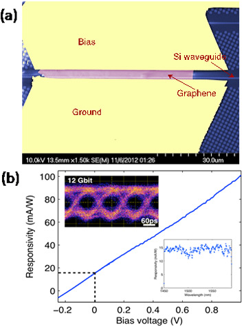
(a) Scanning electron microscopy image of the graphene photodetector, integrated with a silicon waveguide. (b) Responsivity of the photodetector as a function of source-drain bias. Top inset: Undistorted 12 Gbit/s transmission with the graphene detector. Bottom inset: Uniform photo-response is tested from 1,450 nm to 1,590 nm.
Graphene-based photodetectors have attracted strong interest because of their exceptional physical properties, which include an ultra-fast response across a broad spectrum, a strong electron–electron interaction and photocarrier multiplication. However, the weak optical absorption of graphene limits its photo-responsivity. To address this, graphene has been integrated into nanocavities, microcavities, and plasmon resonators; yet, these approaches restrict photodetection to narrow bands. Hybrid graphene–quantum dot architectures can greatly improve responsivity, but at the cost of response speed. In this research project, a waveguide-integrated graphene photodetector was demonstrated that simultaneously exhibits high responsivity, high speed and broad spectral bandwidth. Using a metal-doped graphene junction coupled evanescently to the waveguide, the detector achieves a photoresponsivity exceeding 0.1 A/W together with a nearly uniform response between 1,450 nm and 1,590 nm. Under zero-bias operation, response rates exceeding 20 GHz were achieved, and an instrumentation-limited 12 Gbit/s optical data link was confirmed.
Why Does This Matter?
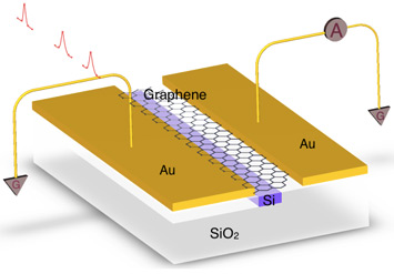
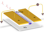
Schematic of a waveguide-integrated photodetector comprised of graphene.
The responsivity is 0.1 A/W, which is comparable to current germanium photodetectors in silicon photonic integrated circuits. The response rates of the device exceed 20 GHz, such that the system performs without distortion in a real 12-Gbit/s optical data link. Further, this graphene light detector shows 16 times higher response than conventional graphene-based photodetectors. These characteristics have established the groundwork for on-chip graphene optoelectronics, which provides a promising solution for efficient on-chip optical networks.
Silicon-based photonic circuits are promising for high-speed computer chips with low power
What Are The Details?
- CFN Capabilities: The CFN Nanofabrication Facility was used to perform advanced fabrication processes that integrated graphene with silicon photonic integrated circuits.
Publication Reference
Chip-Integrated Ultrafast Graphene Photodetector with High Responsivity
X. Gan1†, R.-J. Shiue2†, Y. Gao3, I. Meric1, T. F. Heinz4, K. Shepard1, J. Hone3, S. Assefa5, and D. Englund1,2*
Department of Electrical Engineering, Columbia University, New York, New York 10027, USA
Department of Electrical Engineering and Computer Science, Massachusetts Institute of Technology, Cambridge, Massachusetts 02139, USA
Department of Mechanical Engineering, Columbia University, New York, New York 10027, USA
Department of Physics, Columbia University, New York, New York 10027, USA
IBM T. J. Watson Research Center, Yorktown Heights, New York 10598, USA
†These authors contributed equally to this work.
Nature Photonics 7, 883-887 (2013)
Acknowledgement of Support
The authors thank F. Koppens for discussions. Financial support was provided by the Air Force Office of Scientific Research PECASE (supervised by G. Pomrenke), the DARPA ‘Information in a Photon’ programme (grant no. W911NF-10-1-0416) and by NSF grant DMR-1106225 (T.H.). Device fabrication was partly carried out at the Center for Functional Nanomaterials, Brookhaven National Laboratory, which is supported by the US Department of Energy, Office of Basic Energy Sciences (contract no. DE-AC02- 98CH10886). Device assembly (including graphene transfer) and characterization was supported by the Center for Re-Defining Photovoltaic Efficiency Through Molecule Scale Control, an Energy Frontier Research Center funded by the US Department of Energy, Office of Science, Office of Basic Energy Sciences (award no. DE-SC0001085). R.-J.S. was supported in part by the Center for Excitonics, an Energy Frontier Research Center funded by the US Department of Energy, Office of Science, Office of Basic Energy Sciences under award no. DE-SC0001088.
2014-5166 | INT/EXT | Newsroom