Printing Electronic Parts for Next-Generation Technologies
Custom inks and advanced printing methods enable durable transistors for smart devices
March 11, 2026
By Amber Rose
 enlarge
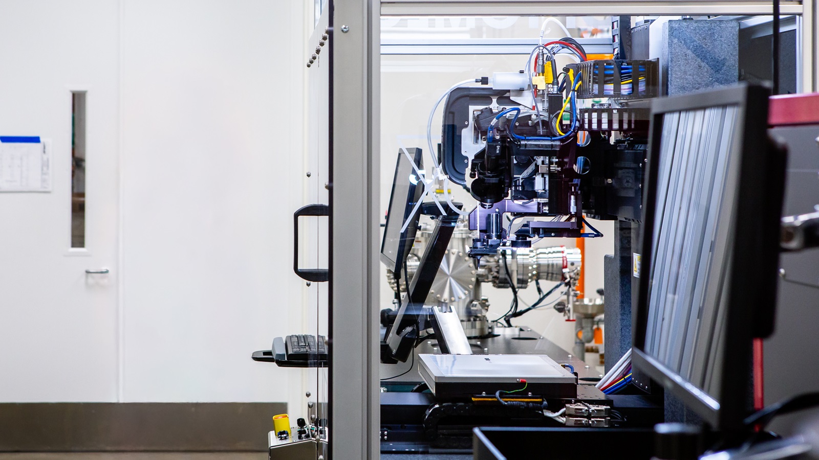
Aerosol jet printer at Argonne used to deposit custom nanoparticle inks and build printed electronic parts for low-power transistor devices. (Image by Argonne National Laboratory.)
Editor’s note: The following press release was originally published by Argonne National Laboratory. Brookhaven lab beamline scientists Evan Musterman, Yang Yang, and Andrew Kiss helped the research team map the shape and elemental makeup of the 3D jet printed microelectronic devices through high-resolution X-ray spectroscopy studies using the Submicron Resolution X-ray Spectroscopy (SRX) beamline at the National Synchrotron Light Source II (NSLS-II), a U.S. Department of Energy (DOE) Office of Science user facility at DOE’s Brookhaven National Laboratory. This new 3D printing technique paves the way for electronic devices that can be made and tested faster than current manufacturing methods. For more information on Brookhaven’s role in this research, contact Denise Yazak (dyazak@bnl.gov, 631-344-6371).
Tiny electronic devices, called microelectronics, may one day be printed as easily as words on a page, thanks to new research from scientists at the U.S. Department of Energy’s (DOE) Argonne National Laboratory. Building on years of progress in printed electronics, the team has shown how to create durable, low-power electronic switches, called transistors, by combining custom inks and a specialized printing process. These switches, which control the flow of electrical current to turn circuits on and off, use very little power, are built to last and show new behaviors not seen in earlier printed devices. This research could help create flexible sensors, smart windows and other new technologies that need reliable, energy-saving electronics.
The scientists used a method called aerosol jet printing, which works like an inkjet printer. But instead of regular ink, it uses specially formulated ink made from nanoparticles. The printer turns the ink into a fine mist and sprays it onto a surface, building up layers to form electronic parts.
Unlike traditional manufacturing, which often requires expensive equipment and high temperatures, aerosol jet printing works at lower temperatures and can print on flexible or even 3D surfaces. This approach makes it easier and faster to develop and test new electronic designs.
To fine-tune these inks, the team used the Center for Nanoscale Materials (CNM) at Argonne, to watch how nanoparticles clump together, see how they change with heat and check the stability and makeup of the dried films — insights that helped improve the ink formulations. They also used the 2-ID-E hard X-ray microprobe at Argonne’s Advanced Photon Source (APS), to map the shape and elemental makeup of the printed devices, complementing high-resolution X-ray spectroscopy studies at Brookhaven’s National Synchrotron Light Source II (NSLS-II). CNM, APS and NSLS-II are all DOE Office of Science user facilities.
A key ingredient in these printed devices is vanadium dioxide. This material is special because it can act like a wire, letting electricity flow, or like an insulator, blocking electricity. This switching ability is important for making electronic circuits and memory devices, which store and process information.
To control the flow of electricity in the transistors, the team used a process called redox gating. In simple terms, this means they use a chemical reaction to add or remove electrons from the vanadium dioxide. By applying a small voltage — less than what is used in a typical battery — they can turn the transistor on or off. This method is less harsh than other techniques, which could damage the material and make devices wear out quickly.
In laboratory tests, the printed transistors operated at voltages as low as 0.4 to 0.5 volts and kept working for more than 6,000 on-off cycles, which is much longer than previous printed devices. The switches also responded quickly, changing states in about one second.
“We chose printing methods for two main reasons,” said Argonne Materials Scientist Yuepeng Zhang. “First, printing enables rapid prototyping and iterative design, which helps us optimize materials and device structures quickly. Second, printed electronics have benefits for device functionality, especially since our devices show a well-modulated current response to voltage, making them suitable for printed logic devices and niche applications.”
When the printed transistor was switched on using a small control signal of 0.5 volts, it allowed about 50% more electricity to flow through it compared to when it was off. In other words, the device could boost the flow of electric current by half with just a tiny amount of power. This shows that the transistor can reliably control electricity using very little energy, which is important for making low-power and flexible electronic devices.
Wei Chen, a chemist from Argonne and the University of Chicago, emphasized the durability of the new devices. “Redox gating is robust and does not damage the materials, so we can run thousands of cycles without issues,” he said. “In previous methods, devices could only run a few times — sometimes just 10 cycles — before failing. Our devices can run thousands of cycles with no problem.”
Right now, these printed transistors are larger and slower than the tiny silicon chips found in most electronics. But this research shows that it is possible to make strong, low-power devices with printing methods.
Chen added, “From my perspective, the next step is logic devices. We’ve been in contact with industry partners interested in testing our devices for logic applications, which are the basic building blocks for computers. That is something I would like to pursue.”
They are also exploring how these printed devices could be used in neuromorphic computing, an area that mimics the way the human brain processes information.
To move printed electronics from the lab to real products, the researchers say more teamwork is needed between scientists and industry. They also believe that artificial intelligence and machine learning could help improve the printing process and make development faster.
“Printing involves many variables to adjust, and machine learning can help us find the best settings more quickly,” Zhang said.
With more research and collaboration, printed hybrid electronics could help make future technology more flexible, affordable and energy efficient.
The results of this research were published in Advanced Materials Technology.
Other contributors to this work include Samuel Miller and Hua Zhou from Argonne; and Evan Musterman, Andrew Kiss and Yang Yang from the National Synchrotron Light Source II at DOE’s Brookhaven National Laboratory. Andrew Erwin and Shiyu Hu were at Argonne when this research is conducted.
This work was primarily supported by the Laboratory Directed Research and Development program at Argonne, with additional support from DOE’s Office of Science, Basic Energy Sciences.
About Argonne’s Center for Nanoscale Materials
The Center for Nanoscale Materials is one of the five DOE Nanoscale Science Research Centers, premier national user facilities for interdisciplinary research at the nanoscale supported by the DOE Office of Science. Together the NSRCs comprise a suite of complementary facilities that provide researchers with state-of-the-art capabilities to fabricate, process, characterize and model nanoscale materials, and constitute the largest infrastructure investment of the National Nanotechnology Initiative. The NSRCs are located at DOE’s Argonne, Brookhaven, Lawrence Berkeley, Oak Ridge, Sandia and Los Alamos National Laboratories. For more information about the DOE NSRCs, please visit https://science.osti.gov/User-Facilities/User-Facilities-at-a-Glance.
About the Advanced Photon Source
The U. S. Department of Energy Office of Science’s Advanced Photon Source (APS) at Argonne National Laboratory is one of the world’s most productive X-ray light source facilities. The APS provides high-brightness X-ray beams to a diverse community of researchers in materials science, chemistry, condensed matter physics, the life and environmental sciences, and applied research. These X-rays are ideally suited for explorations of materials and biological structures; elemental distribution; chemical, magnetic, electronic states; and a wide range of technologically important engineering systems from batteries to fuel injector sprays, all of which are the foundations of our nation’s economic, technological, and physical well-being. Each year, more than 5,000 researchers use the APS to produce over 2,000 publications detailing impactful discoveries, and solve more vital biological protein structures than users of any other X-ray light source research facility. APS scientists and engineers innovate technology that is at the heart of advancing accelerator and light-source operations. This includes the insertion devices that produce extreme-brightness X-rays prized by researchers, lenses that focus the X-rays down to a few nanometers, instrumentation that maximizes the way the X-rays interact with samples being studied, and software that gathers and manages the massive quantity of data resulting from discovery research at the APS.
This research used resources of the Advanced Photon Source, a U.S. DOE Office of Science User Facility operated for the DOE Office of Science by Argonne National Laboratory under Contract No. DE-AC02-06CH11357.
Argonne National Laboratory seeks solutions to pressing national problems in science and technology by conducting leading-edge basic and applied research in virtually every scientific discipline. Argonne is managed by UChicago Argonne, LLC for the U.S. Department of Energy’s Office of Science.
The U.S. Department of Energy’s Office of Science is the single largest supporter of basic research in the physical sciences in the United States and is working to address some of the most pressing challenges of our time. For more information, visit https://www.energy.gov/science/office-science.
2026-22857 | INT/EXT | Newsroom