Gold in Limbo Between Solid and Melted States
By capturing the laser-induced structural changes happening in polycrystalline gold thin films over time, scientists determined that melting does not occur uniformly—a finding that could have implications to laser micromachining of precision parts
March 2, 2020
 enlarge
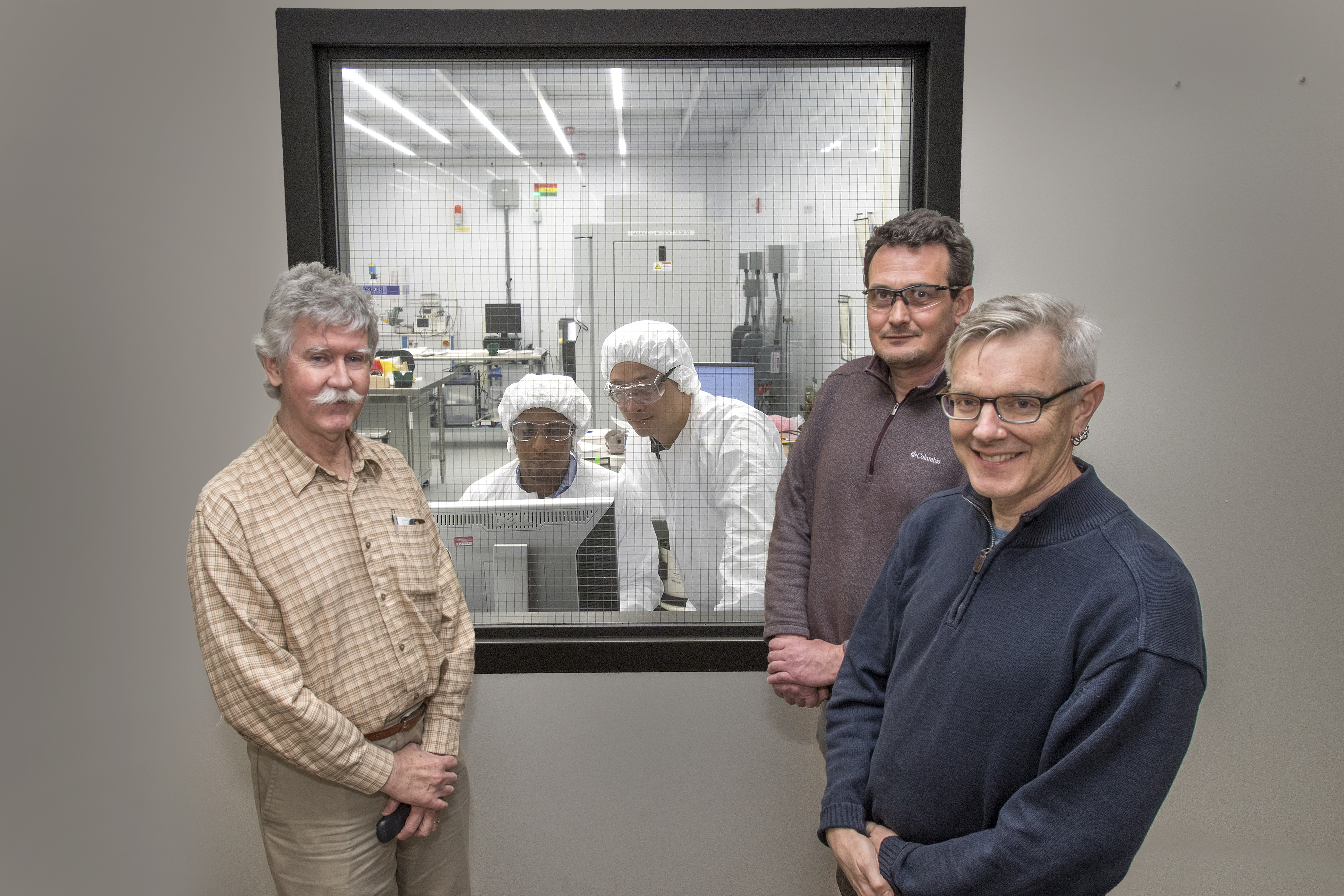
Brookhaven Lab physicists (from left to right) Ian Robinson, Tadesse Assefa, Ming Lu, Emil Bozin, and Simon Billinge at the Center for Functional Nanomaterials cleanroom, where they fabricated polycrystalline gold films of 50-, 100-, and 300-nanometer thickness. The team used time-resolved x-ray diffraction to understand the mechanism of melting in films excited by a laser that emits optical pulses with an extremely short duration. Their analysis of the x-ray diffraction images revealed that melting (induced by the laser) starts in one place and then moves into another location.
UPTON, NY—If you heat a solid material enough, the thermal energy (latent heat) causes the material’s molecules begin to break apart, forming a liquid. One of the most familiar examples of this phase transition from a well-ordered solid to less-ordered liquid state is ice turning into water.
Though melting is a fundamental process of matter, scientists have not been fully able to understand how it works at a microscopic level, owing to the lack of research capabilities with sufficient time resolution. However, the advent of x-ray free-electron lasers (XFELs) in the past decade is making the study of the mechanism of melting, as well as other ultrafast atomic-scale dynamics, possible. These instruments use free (unbound) electrons to generate femtosecond (one-quadrillionth of a second) pulses of light in the x-ray energy region. Compared with x-ray synchrotrons, XFELs have x-ray pulses of a much shorter duration and higher intensity.
 enlarge
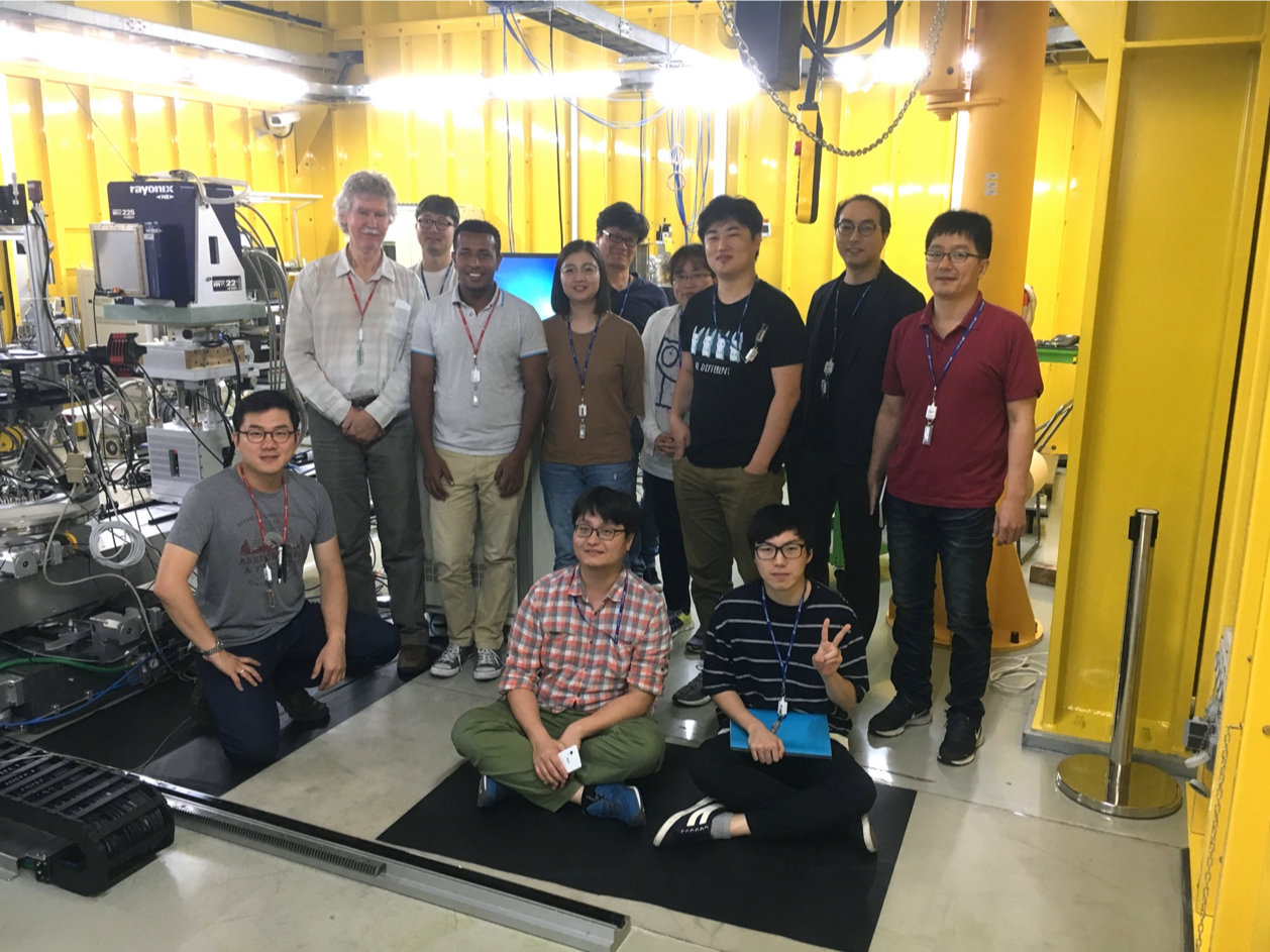
Part of the team at the Pohang Accelerator Laboratory X-ray Free-Electron Laser (PAL-XFEL) in South Korea, where they conducted their experiments. This team is the second international group to use this facility, which is one of five of its kind in the world. The other XFEL facilities are located in the United States (at SLAC National Accelerator Laboratory), Germany, Japan, and Switzerland.
Now, a team of international scientists has used one of these instruments—the Pohang Accelerator Laboratory XFEL (PAL-XFEL) in South Korea—to monitor the melting of nanometer-thick gold films made up of lots of very tiny crystals oriented in various directions. They used an ultrashort x-ray pulse (“probe”) to monitor the structural changes following the excitation of these polycrystalline gold thin films by a femtosecond laser (“pump”), which induces melting. When the x-ray pulse strikes the gold, the x-ray beam gets diffracted in a pattern that is characteristic of the material’s crystal structure. By collecting x-ray diffraction images at different pump-probe time delays on picosecond (one-trillionth of a second) scales, they were able to take “snapshots” as melting began and progressed in the gold thin films. Changes in the diffraction patterns over time revealed the dynamics of crystal disordering. The scientists selected gold for this study because it diffracts x-rays very strongly and has a well-defined solid-to-liquid transition.
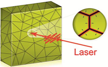
An illustration of grain boundary locations (points where lines intersect) in a polycrystalline gold thin film. The zoomed-in view shows how a melt front created at these boundaries propagates into the grains after the film is excited with an optical laser.
The x-ray diffraction patterns revealed that melting is inhomogeneous (nonuniform). In a paper published online in the Jan. 17 issue of Science Advances, scientists proposed that this melting likely originates at the interfaces where crystals of different orientations meet (imperfections called grain boundaries) and then propagates into the small crystalline regions (grains). In other words, the grain boundaries start melting before the rest of the crystal.
“Scientists believed that melting in polycrystalline materials occurs preferentially at surfaces and interfaces, but before XFEL the progression of melting as a function of time was unknown,” said co-corresponding author Ian Robinson, leader of the X-ray Scattering Group in the Condensed Matter Physics and Materials Science (CMPMS) Division at the U.S. Department of Energy’s (DOE) Brookhaven National Laboratory. “It was known that the laser generates “hot” (energetic) electrons, which cause melting when they transfer their energy to the crystal. The idea that this energy transfer process happens preferentially at grain boundaries and thus is not uniform has never been proposed until now.”
“The mechanism of laser-induced melting is important to consider for micromachining of precision parts used in aerospace, automotive, and other industries,” added first author Tadesse Assefa, a postdoc in Robinson’s group. “The way the laser couples to the material is different depending on the pulse duration of the laser. For example, the ultrashort pulses of femtosecond lasers seem to be better than the longer pulses of nanosecond lasers for making clean cuts such as drilling holes.”
For their experiment, the scientists first fabricated thin films of varying thickness (50, 100, and 300 nanometers) at the Center for Functional Nanomaterials (CFN)—a DOE Office of Science User Facility at Brookhaven. Here, in the CFN Nanofabrication Facility, they performed electron-beam evaporation, a deposition technique that uses electrons to condense the desired material onto a substrate. The ultraclean environment of this facility enabled them to create gold films of uniform thickness over a large sample area.
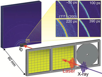
A schematic of the experimental setup for the time-resolved x-ray diffraction studies on the polycrystalline gold thin films. The sample is mounted perpendicular to the XFEL beam. A laser "pump" excites the sample, and then an x-ray pulse "probe" monitors the laser-induced changes at different time delays. The inset shows the x-ray diffraction patterns generated for the 300-nanometer film 50 picoseconds before and 100, 220, and 390 picoseconds after laser excitation.
At PAL-XFEL, they conducted time-resolved x-ray diffraction on these films over a range of laser power levels. Software developed by staff in Brookhaven Lab’s Computational Science Initiative handled the high-throughput analysis of the terabytes of data generated as a detector collected the diffraction pattern images. The team then used software developed by scientists at Columbia Engineering to convert these images into linear graphs.
The plots revealed a double peak corresponding to a “hot” region undergoing melting (intermediate peak) and a relatively “cold” region (the rest of the crystal) which has yet to receive the latent heat of melting. Through electron coupling, heat goes to the grain boundaries and then conducts into the grains. This uptake of latent heat results in a band of melting material sandwiched between two moving melt fronts. Over time, this band becomes larger.
“One melt front is between a solid and melting region, and the other between a melting and liquid region,” explained Robinson.
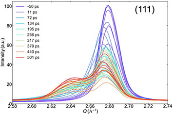
X-ray diffraction intensity profiles for the 300-nanometer-thick film measured at various time delays (color-coded lines), ranging from 50 picoseconds before laser excitation at an optimal power level to 501 picoseconds after excitation. From this double peak structure of a sharp crystal powder peak and a broader intermediate peak, scientists were able to infer that the film does not all melt uniformly. They also generated profiles for the thinner films, where melting happens more quickly and requires less laser energy.
Next, the team plans to confirm their two-front model by reducing the size of the grains (thereby increasing the number of grain boundaries) so they can reach the end of the melting process. Because melting occurs as a wave traversing the crystal grains at a relatively slow speed (30 meters per second), it takes longer than the timing range of the instrument (500 picoseconds) to cross big grains.
They would also like to look at other metals, alloys (mixtures of several metals or a metal combined with other elements), and catalytically relevant materials, in which grain boundaries are involved in chemical reactions.
“This study represents the very beginning of how we build an understanding of the mechanism of melting,” said Assefa. “By performing these experiments using different materials, we will be able to determine if our model is generalizable.”
The other collaborating institutions are University College London, Sogang University, and Pohang University of Science and Technology.
Brookhaven National Laboratory is supported by the U.S. Department of Energy’s Office of Science. The Office of Science is the single largest supporter of basic research in the physical sciences in the United States and is working to address some of the most pressing challenges of our time. For more information, visit https://energy.gov/science.
Follow @BrookhavenLab on Twitter or find us on Facebook.
2020-17020 | INT/EXT | Newsroom