Percy Zahl: Mapping Materials at the Nanoscale
October 23, 2012
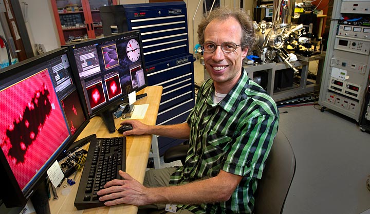
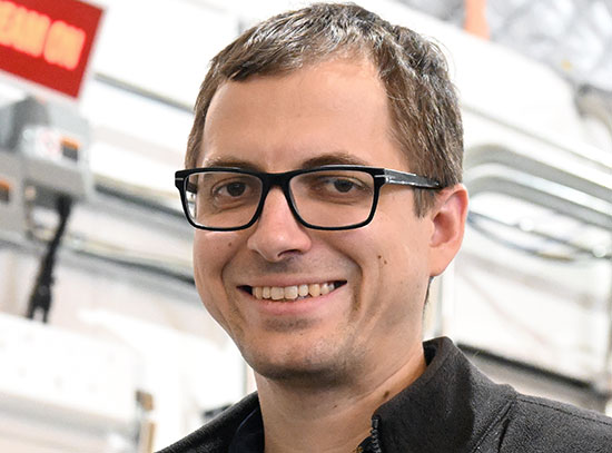
Percy Zahl in the lab at Brookhaven's Center for Functional Nanomaterials where he uses scanning tunneling microscopy and spectroscopy along with the software package he developed to map the surface of nanomaterials measured in billionths of a meter — with atomic-scale, pinpointed accuracy.
In 1804, Lewis and Clark set out to explore more than two million square kilometers of land west of the Mississippi River. Now in 2012, Percy Zahl of Brookhaven Lab's Center for Functional Nanomaterials (CFN) is exploring the surface of materials measured in billionths of a meter — with atomic-scale, pinpointed accuracy. Zahl has written 300 thousand lines of computer software that he and scientific researchers use to create stunning images and multidimensional maps of innovative nanomaterials as they chart the topography of these surfaces, as well as their electrical properties. Next week, the American Vacuum Society (AVS) will recognize Zahl for his support of these monumental yet nano-sized explorations.
The AVS is a professional society for people who work toward advances in basic science, technology development, and commercialization of materials, interfaces, and processing. The society will present Zahl with its George T. Hanyo Award during its 59th International Symposium & Exhibition that will be held in Tampa, Fl. beginning on October 28. Zahl was selected for the award because of his outstanding leadership in the development of state-of-the-art, open-source software — called GXSM or the Gnome X Scanning Microscopy project — for data acquisition and analysis in scanning probe microscopy and spectroscopy.
“I am honored to receive this prize from the AVS for my continuous dedication to the GXSM software project,” said Zahl. “GXSM has been an ongoing project for 16 years, so I really appreciate this recognition.”
Charting the “Turf”
When charting materials at the nanoscale, tape measures and hand-held compasses are of no use. At Brookhaven, researchers can use scanning tunneling microscopy (STM) and spectroscopy (STS) to look at individual atoms and molecules and generate topographical maps of nanomaterials. STM and STS were developed in the early 1980s at IBM Zurich, where Zahl later worked as a postdoc.
A nanoscale-map Zahl and his group leader Peter Sutter acquired using scanning tunneling microscopy (STM) in February 2003 at the Colorado School of Mines before they arrived at Brookhaven. Likely to be the world's highest-resolution, single scan of a silicon surface, the original STM image contains data from 30,000 by 30,000 points from an area just 0.5 a micrometer squared — that's one half of one millionth of a meter in width and one half of one millionth of a meter in height. Right: A more close-up look of the same map, showing detailed atomic structures.
To understand how STM and STS work, start by thinking of a record player — only with a needle-like probe tip just a few atoms thick that doesn't drag along the record's surface, but instead hovers just above. First, Zahl said a sample is placed into a vacuum chamber that is prepared, cleaned, and cooled to 5 Kelvin (-450 degrees Fahrenheit). At that frigid temperature, both the sample and instrument remain über clean and stable. Thanks to a phenomenon called “tunneling” that occurs in the ultra-small quantum world, a current of electrons can tunnel, or flow, between the probe's tip and the sample as long as physical contact is not made. Determining this current is an extremely sensitive way to measure the distance between the tip and sample.
The probe then takes measurements point by point as it scans the material's surface — traversing across, shifting down, traversing again, and so on. The computer system and machinery work to maintain a constant distance and tunneling current between the tip and the surface. If the needle reaches a “dip” in the surface, the needle shifts down. If needle reaches a rise, it shifts up.
Meanwhile, the digital signal processing system that does the work of positioning the tip acquires data that is then sent to a computer that runs Zahl's GXSM software to assemble the data into images and maps of the material's surface.
“Not only does this system allow scientists to explore the nano world, it also allows for manipulation by moving around individual atoms and molecules,” Zahl explained.
Researchers from the Brookhaven's Basic Energy Sciences Directorate and around the world bring their own samples and experiments to the CFN for prospecting at the STM facility. Zahl typically hosts these researchers for sessions that last about two weeks.
“Sometimes tips break, sometimes things shift unexpectedly and the images are unusable,” Zahl said. “STM is like driving a race car — anyone can do it, but doing it safely and well enough to finish a long race requires a lot experience.”
It's his experience and the art of large scale programming Zahl developed that enabled him and his group leader Peter Sutter to set what is very likely the world record for the highest resolution scan of a silicon germanium sample. Their scan contains 30,000 by 30,000 points and they completed it successfully while at the Colorado School of Mines, before they came to Brookhaven.
“I wanted to make available the best open-source software package for scanning tunneling microscopy.”
— Percy Zahl
Not Coded in a Day
Zahl began working on the GXSM software package around 1996. Since December 2000, the open-source software has been available under the GNU General Public License, which means that people can download the entire package — including accessible source code — to use and customize for free. Zahl's collaborator Thorsten Wagner of the Institute for Experimental Physics in Austria is also a project administrator who helps support people who use the software package today at more than 60 institutions in 20 different countries. Zahl also maintains a forum online where he and users discuss the project, new ideas, and future developments.
“I got interested in this because I was working on my thesis with a group in Germany that had microscopes, but didn't have the money for a full-scale commercial system,” Zahl explained. “We got together everything we needed and the software part of it became a hobby. I wanted to make available the best open-source software package for scanning tunneling microscopy.
“The software is future-proof, because I designed it modularly to adapt with new plug-ins and add-ons,” Zahl added. “We often need to make the software do something new or work with next generation STM techniques and computer hardware. I built it so that the only limitation is a computer's hardware. If a computer can take it, the software can handle it.”
Zahl earned a Ph.D. in physics at the Institut für Festkörperphysik, Universität Hannover — the Institute for Solid State Physics at Hannover — in Germany in 2000. He worked as a postdoc in the Physics Department at the Colorado School of Mines from 2001 to 2003, and then as an IBM postdoc fellow at IBM Zürich from 2003 to 2005. He arrived at Brookhaven Lab's Center for Functional Nanomaterials as an associate scientist in 2005.
In addition to supporting the Lab's STM program at the CFN, Zahl rides his bicycle any chance he gets. He rides to the Lab from his home in Rocky Point whenever weather permits it. He's also a member of the Green Arm Bandits cycling team. With the team and fellow riders — including several fellow BNLers — Zahl has pedaled more than eight thousand miles in 2012 alone, exploring the tri-state area, New England, and some of the biggest Alpine passes during a short trip he took to Switzerland and Italy this past summer.
2012-3318 | INT/EXT | Newsroom


