Research Highlight: Nanocrystals Within Nanowires
innovation at CFN
April 21, 2016
What is the scientific achievement?
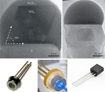
Top: High-resolution electron microscopy images of a nickel silicide rhombic nanocrystal embedded in a silicon nanowire prepared with a gold silicide catalyst. The images demonstrate the intimate interactions that arise at the interfaces of these nanomaterials. Bottom: The physical properties of such complex nanosystems could be used in next-generation photodetectors, lasers, and transistors.
An international collaboration led by the University of Cambridge and IBM has demonstrated a method to create novel nanowires that contain embedded nanocrystals. This approach is a modification of the classic vapor-liquid-solid crystal growth method in which a liquid-phase catalyst is used to decompose an incoming gas-phase source and to mediate the deposition of the solid growing nanowire. In this work, a bimetallic catalyst is used. Through appropriate thermal treatment, a solid silicide structure can crystallize within the liquid catalyst and then attach the nanowire to the solid silicon in a controlled epitaxial fashion.
Why does this achievement matter?
Semiconducting nanowires have a wide range of existing and potential applications in optoelectronic materials, from single-electron transistors and tunnel diodes, to light-emitting semiconducting nanowires, to photoconductors, to semiconductor lasers, and energy-harvesting devices. The ability to control the growth of crystalline structures at the nanoscale could lead to new classes of nanoscale devices.
What are the details?
This movie, recorded at the CFN environmental transmission electron microscope, shows incorporation of a NiSi2 nanocrystal into a Si nanowire. First, the nanoparticle becomes attached to the top of the nanowire, in a process similar to that shown in the series of still images. Then, more silicon is grown to surround the nanocrystal. The movement of the catalytic droplet (dark) is visible during the entire process. The movie was recorded at 400 frames per second and 550°C while flowing 5×10⁻⁵ Torr Si2H6, and it is speeded up by 2×.
CFN Capabilities: High-spatial-resolution, aberration-corrected transmission electron microscopy at CFN’s Electron Microscopy Facility was used to image the complex nanomaterials. A first-of-its-kind direct electron detector was used to obtain high-temporal-resolution images of the fabrication process.
Publication Reference
“Synthesis of nanostructures in nanowires using sequential catalyst reactions”
F. Panciera1,2, Y.-C. Chou2,3,4, M.C. Reuter2, D. Zakharov4, E.A. Stach4, S. Hofmann1, and F.M. Ross2
1 Department of Engineering, Cambridge University, Cambridge, CB3 0FA, United Kingdom
2 IBM Research Division, T.J. Watson Research Center, Yorktown Heights, New York, 10598
3 Department of Electrophysics, National Chiao Tung University, Hsinchu City, Taiwan
4 Center for Functional Nanomaterials, Brookhaven National Laboratory, Upton, New York, 11973
Nature Materials 14, 820–825 (2015)
Acknowledgement of Support
This research was supported by the National Science Foundation under Grants No. DMR-0606395 and 0907483 (Y.-C.C.), ERC Grant 279342: InSituNANO (F.P. and S.H.), the National Science Council of Taiwan under Grant No. NSC-101-2112-M-009-021-MY3 (Y.-C.C.), the Center for Interdisciplinary Science under the MOE-ATU project for NCTU (Y.-C.C.), and the Center for Functional Nanomaterials, Brookhaven National Laboratory, which is supported by the US Department of Energy, Office of Basic Energy Sciences, under contract DE-AC02-98CH10886 (D.Z. and E.A.S.). The authors acknowledge A. Gamalski for assistance with high-resolution imaging, C. Czarnik for assistance with image processing, and A. Ellis for technical support.
2016-6339 | INT/EXT | Newsroom