Q&A with CFN User Don DiMarzio
December 6, 2016
Don DiMarzio is an engineering fellow at Northrop Grumman and a senior scientist within the company’s advanced research, development, design, and demonstration group NG Next, where he studies nanomaterials and radio-frequency metamaterials. He is also an adjunct professor at Stony Brook University, where he teaches a nanotechnology class. Since March 2016, he has been using the advanced characterization labs at the Center for Functional Nanomaterials (CFN)—a U.S. Department of Energy (DOE) Office of Science User Facility at Brookhaven Lab—primarily to investigate nanostructures whose self-assembly is directed through DNA scaffolds. CFN physicist Oleg Gang has been developing this DNA-based technique for several years.
Northrop Grumman is typically known for building aircraft, such as the U.S. Air Force’s B-2 stealth bomber, as well as unmanned autonomous aircraft and satellites. How does basic research come into play?
About two years ago, Tom Vice, corporate vice president and president of Northrop Grumman Aerospace Systems, began discussing with his leadership team how to reconstitute the basic research activity that had existed in various forms earlier in the company’s history. NG Next, which includes basic research, applied research and technology development, advanced design, and rapid prototyping, emerged from these discussions. The goal of NG Next is to position Northrop Grumman at the cutting edge of science and technology and to attract the best and brightest young talent.
NG Next’s basic research group is led by Tom Pieronek, vice president of basic research. The group has eight thrusts or topic areas relevant to the aerospace industry. One of these topics is nanomaterials, which is the focus of the Nanomaterials Group, led by Jesse Tice. I belong to this group. Other thrusts within the basic research group include semiconductor materials, plasmonics, and cognitive autonomy. The charter of our basic research organization is to do real science that is nonproprietary and publishable, in collaboration with the nation’s top universities and government labs. Any fundamental new discoveries that we think are promising may be transferred over to our applied research and prototyping groups within NG Next.
The Center for Functional Nanomaterials (CFN) is one of five U.S. Department of Energy Nanoscale Science Research Centers and is among the many nanoscale facilities located at universities across the United States. What influenced your decision to submit a user proposal to CFN?
After I got my PhD in solid-state physics, I did a postdoc at Brookhaven’s National Synchrotron Light Source (NSLS) in the late 1980s and really enjoyed working at Brookhaven. After my postdoc, I became a scientist at the Grumman Corporate Research Center in Bethpage, NY, but continued my collaborations with Brookhaven on and off throughout the years.
When Northrop Grumman leadership began planning for the new basic research group last year, I got involved. Part of my planning and development work for the group included helping to organize workshops—one in nanomaterials and the other in radio-frequency metamaterials—at our regional headquarters in southern California. For these invite-only workshops, the goal was to learn what was at the cutting edge in research, where we should focus our efforts, and who we could collaborate with.
Our Nanomaterials Workshop provided a broad perspective on cutting-edge research, from nanomaterials synthesis and structures fabrication through fundamental properties and applications. One area that showed great potential was in nanoparticle self-assembly, and one of the major players in that field is the CFN. Although I had been working with various nanotechnologies before the establishment of NG Next, the CFN was either not established yet or our research was both applied and highly proprietary. But with the establishment of the basic research group within NG Next, it became clear that there was a definite opportunity for collaboration, especially considering that the way CFN is set up aligns with NG Next’s charter to publish, make presentations, and collaborate.
When I learned about CFN physicist Oleg Gang’s work on exploiting DNA to direct the self-assembly of nanoparticles, I became very intrigued. I was particularly impressed with the strength and flexibility of this DNA origami scaffolding to fabricate a wide range of structures relevant for device and materials applications, and the ability to transition these assemblies from “soft” to “hard” while preserving key functionalities. Northrop Grumman sees this work as a potentially ground-breaking area that may lead to revolutionary new fabrication capability for everything from sensor systems to structural composites.
While most of NG Next’s basic research group is in California, I am here on Long Island (at our Bethpage facility), so CFN is conveniently located near where I work and live. The group in California is currently building out its own labs that will be separate from our traditional applied laboratories. As an existing facility with state-of-the-art equipment and expertise in nanomaterials synthesis, device fabrication, and advanced characterization, CFN was the perfect complement to our West Coast research operations.
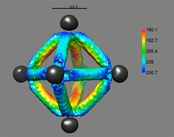 enlarge
Gold nanoparticles are coordinated by DNA origami octahedron into the prescribed cluster, as obtained from the 3D transmission electron microscopy reconstruction (based on Y. Tian et al. Nature Nanotechnology 10, 637–644, 2015).
Are you working on any other projects at CFN besides the directed self-assembly?
In nanomaterials research, I am supporting principal investigators who are using CFN’s advanced characterization tools, particularly those in microscopy, to look at cutting-edge 2D materials like tin selenide (SnSe) and black phosphorous, in collaboration with our university partners.
For our nanomaterials work, I am also collaborating with an NG Next group involved in plasmonics research, leveraging our DNA assembly work to fabricate new and unique optical structures.
What are some of the characterization techniques you use at CFN?
To probe the composition of the DNA-based nanostructures, we focus on small-angle x-ray scattering (SAXS) and transmission electron microscopy (TEM). To probe the chemical states of 2D materials and devices, we use energy-dispersive x-ray spectroscopy and electron energy-loss spectroscopy. In addition to these traditional microscopy techniques, we employ aberration-corrected low-energy electron microscopy (LEEM) and angle-resolved photoemission spectroscopy (ARPES) for some of our 2D materials. This latter technique is important because the band structure, or electronic energy levels, of 2D materials often has directional dependence.
Your work at CFN sounds like it could also benefit from the advanced characterization methods at the National Synchrotron Light Source II (NSLS-II). Are you collaborating with NSLS-II or do you have plans to?
Plans are in the works for experiments at the NSLS-II, building on our current efforts at the CFN. We will be working with CFN scientists Dario Stacchiola and Jerzy Sadowski on the new LEEM/ARPES system during its commissioning in January, and we are evaluating the use of synchrotron SAXS for large-volume data acquisition from nanomaterials for additive manufacturing.
Our leadership is very supportive of our interactions with Brookhaven’s DOE Office of Science User Facilities and would like to solidify relationships for the long term.
How has it been coming back to Brookhaven more than 30 years later?
Even though I work for Northrop Grumman, I feel like I am part of the family here at CFN. I am working at CFN pretty much every day. From the start, CFN leadership has been very accommodating. They helped us get rapid access while we started negotiations on our CRADA [cooperative research and development agreement] and submitted our long-range user proposals for the directed assembly and 2D materials projects.
Since I arrived, CFN staff scientists have been very helpful with training on laboratory equipment such as the SAXS, TEM, and scanning TEM (STEM) systems. The CFN group leads have been particularly helpful in facilitating timely sample preparation, such as that with the focused-ion beam, and with scheduling the use of characterization tools.
You mentioned you are at CFN basically every day. What keeps you coming back?
I feel like a kid in a candy shop here. Everyone who works here is passionate about what they do, so coming in every day is something I look forward to. I have my own spare office, close to the group leaders who I am working with. Although I primarily work with Oleg, I get to interact with many other staff scientists and postdocs, not only through my research but also through my volunteer work at CFN. I am the elected vice chair of the CFN Users’ Executive Committee and co-chair of the 2017 NSLS-II & CFN Joint Users’ Meeting.
How did you become interested in nanomaterials?
Years ago, I was doing applied research in photocatalysis involving the use of titanium dioxide nanoparticles to create self-decontaminating surfaces—a DARPA [Defense Advanced Research Projects Agency] project. Subsequently, I got involved in developing lightweight carbon nanotube based electrical cables for Department of Defense applications. The carbon nanotube work is ongoing at Northrop Grumman, with applications for space systems and air platforms. Although these applications are important, my turn to basic research was rooted in the NG Next vision to investigate fundamental phenomena that will enable new game-changing technologies that will have applications to both Northrop Grumman’s traditional customers and future technology marketplaces.
2016-6766 | INT/EXT | Newsroom


